
Xuemin Zhang, Changling Yan, Jinghang Yang, Chao Pang, Yunzhen Yue, Chunhong Zeng, Baoshun Zhang. Vertical Schottky ultraviolet photodetector based on graphene and top–down fabricated GaN nanorod arrays[J]. Journal of Semiconductors, 2022, 43(6): 062804
- Journal of Semiconductors
- Vol. 43, Issue 6, 062804 (2022)
Abstract
1. Introduction
GaN has been widely used in the fabrication of ultraviolet photodetectors (UV PDs) because of its direct wide bandgap of 3.4 eV and excellent thermochemical stability[
In this work, the top–down fabrication of GaN nanorods was realized by dry and wet etching of GaN. Further, graphene–GaN nanorod vertical Schottky ultraviolet detectors were manufactured and measured. Excellent photoelectric properties, such as light response rate and specific detection rate, have been obtained.
2. Experimental
Two kinds of GaN epitaxial layers were grown on c-plane sapphire. Where 2 μm GaN thin film was used to characterize the etching rate of dry etching, optimize the wet etching process and measure the photoluminescence spectrum. A 500 nm n–-GaN /1 μm n+-GaN structure was used to fabricate a vertical Schottky ultraviolet detector. The doping concentrations of the n+-GaN and n–-GaN were about 5 × 1018 cm–3 and 2 × 1016 cm–3, respectively.
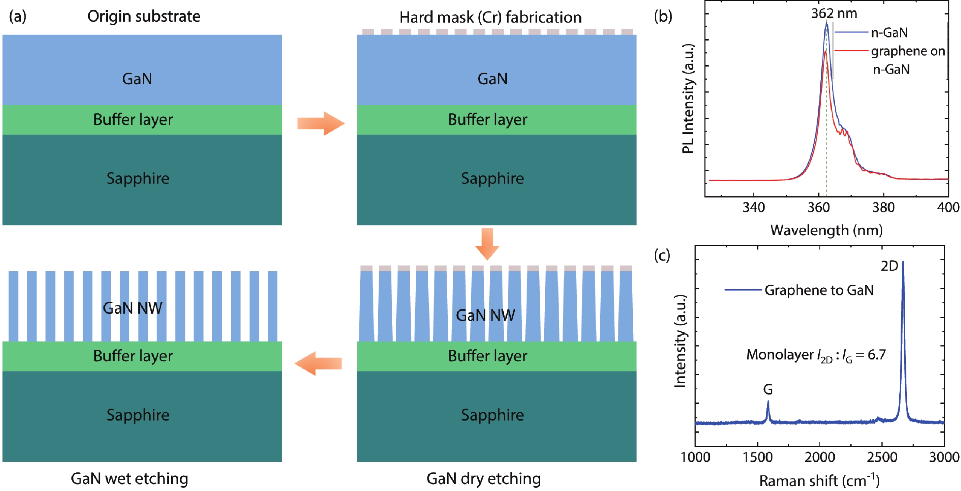
The top–down structure of GaN nanorods was fabricated by the GaN dry and wet etching process. The process diagram is shown in Fig. 1(a). First, the Cr mask was patterned by lithography and ion beam etching (IBE). Second, GaN was etched by inductively coupled plasma (ICP) etching equipment. Finally, wet etching by tetramethylammonium hydroxide (TMAH) solution was used to eliminate the sidewall damage induced by dry etching and form the nanorod’s array structure.
![]()
Figure 1.(Color online) (a) The process schematic diagram of the preparation of GaN nanorods. (b) The PL spectra of GaN before and after graphene transfer. (c) The Raman spectra of graphene grown on copper foil.
The morphology of nanorod arrays was observed by scanning electron microscopy (SEM). The quality of GaN and graphene was evaluated by photoluminescence (PL) and Raman spectroscopy, respectively. Fig. 1(b) shows the PL spectra of GaN before and after graphene transfer. Strong near-band edge emission of GaN substrate indicates fewer defects. The peak at 362 nm coincides with the bandgap of GaN about 3.4 eV. When the graphene was transferred to the GaN substrate, the intensity of the PL peak decreased. The attenuation of PL intensity after graphene transfer happens because graphene also has an amount of light absorption in the ultraviolet region (about 5% per layer at 360 nm)[
For photodetector fabrication, the photolithography for nanometer-level nanorods was performed by electron beam photolithography (EBL). An ohmic contact layer (Ti/Al/Ni/Au, 30/130/50/150 nm) was fabricated on the surface of n+-GaN and annealed at N2 environment (850 °C for 30 s). Then, SiO2 isolation layer (200 nm) was formed around the n–-GaN mesa by plasma enhanced chemical vapor deposition (PECVD) and reactive ion etching (RIE) process. Graphene transfer, photolithography, O2 plasma etching, and H2 annealing at 450 °C were carried out to cover the exposed n–-GaN surface with graphene. The cyclic Schottky electrode (Ni/Au, 50/100 nm) was formed on the peripheral graphene.
Electrical transport measurements were implemented using the Keithley2636A dual-channel digital source meter. A semiconductor laser of 365 nm was used to detect the light response related to the UV wavelength.
3. Results and discussions
The final morphology of GaN nanorods was determined by the corrosion rate of TMAH wet etching. The corrosion rate was affected by solution concentration and temperature. We observed the basic process of GaN nanorods formation by SEM at different etching time. As shown in Fig. 2(a)–2(d), the corrosion time is 3, 5, 10, and 15 min, respectively. It can be seen that the OH– ion in TMAH reacts preferentially with the atoms on the sidewall of the nanorod. The Ga and N atoms dissolve into the solution to form reactants. Because the surface atoms on the sidewalls of the nanorods have open bonds (the dangling bonds are very dense), the sidewall etching rate for this step will be very fast and continue until it reaches the nonpolar m-plane
![]()
Figure 2.The basic process of GaN nanorod formation by SEM at different etching time: (a) 3, (b) 5, (c) 10, (d) 15, (e) 17, and (f) 22 min.
Through experimental exploration, we obtained more optimized TMAH wet etching conditions. TMAH∶H2O was 1∶3, water bath temperature was 80 °C, and corrosion time was 17 min. Then, a GaN nanorod array with ideal morphology was obtained. The SEM measurement results are shown in Fig. 2(e). The diameter of the nanorods is about 335 nm and the height is about 1.14 μm. Although the non-polar m- plane of the sidewall of GaN nanorods has a lower etching rate compared with other planes, it can also be etched in the TMAH solution for a long time. As a result, the diameter of the nanorods was further reduced to a minimum of 78 nm (Fig. 2(f)) as corrosion time continued to increase.
A graphene–GaN nanorod array heterojunction ultraviolet detector was fabricated. Fig. 3(a) shows the cross–sectional structure of the device, with graphene in contact with n–-GaN nanorods forming Schottky structures and n+-GaN in contact with metal electrodes forming ohmic contacts. Fig. 3(b) is an optical microscope image of the device structure. The square region in the middle is the main light–sensitive region of the device. The area was designed between 100 × 100 μm2 and 300 × 300 μm2. The inset is an SEM image of the GaN nanorods. The size of nanorod arrays was consistent with the design value with the diameter of 500 nm and interval of 300 nm. The I–V characteristics of graphene–GaN nanorods photodetectors in darkness and light are compared as shown in Figs. 3(c) and 3(d). With bias varying from –5 to 5 V, Fig. 3(c) shows a significant increase in photocurrent when illuminated with a 365 nm UV light source as compared with darkness.Iphoto : Idark is about 100. The inset of Fig. 3(c) shows that the ideality factor and barrier height were 1.42 and 0.73 eV at the darkness, respectively. It can be seen that the device has excellent detection ability in the band of 365 nm. Fig. 3(d) shows the I–V curve of the y–logarithmic transformation at 100% laser power in the dark and under ultraviolet light. Asymmetric I–V curves show that the Schottky junction has a rectifying behavior in the dark.
![]()
Figure 3.(Color online) (a) The cross-sectional structure of the graphene–GaN nanorod array heterojunction ultraviolet detector. (b) An optical microscope image of the device structure, and the inset is an SEM image of GaN nanorods. (c, d) The
To study the periodicity and sensitivity of the detector to ultraviolet light, we test the switching frequency characteristics of the device. Fig. 3(e) shows the variation of current with time at the drain voltage (VDS) of –5 V under the cyclic ultraviolet illumination of the detector. The band of ultraviolet light was 365 nm and the period was 0.1 s. In a light switching cycle, the photocurrent increased rapidly and then stabilized after reaching the peak. When the light was turned off, the photogenerated carriers gradually fell from the conduction band to the valence band, and the photocurrent decreased rapidly until all of the photogenerated carriers were exhausted. As can be seen from the changes of detector current during the four UV illumination periods in Fig. 3(e), the photoresponsivity of the detector has excellent periodicity and stability. For the sensitivity of the detector, the rise time (τr) was measured from 10% to 90% of the signal peak value. The decay time (τf) was from 90% to 10%[
Fig. 4(a) shows the band structure of the graphene–GaN nanorod array heterostructure. When graphene was exposed to GaN nanorods, electrons from GaN nanorods near the heterojunction interface flow into graphene. This happens because the Fermi level of GaN nanorods is higher than graphene[
![]()
Figure 4.(Color online) (a) The band structure of the graphene–GaN nanorod array heterostructure. (b) A curve of device photoresponsivity as bias voltage changes. (c) The bias voltage and light power as a function of
Photoresponsivity (R) is one of the important parameters of the photodetector. It is defined as the ratio of the photocurrent output to the incident light power over the active region of the detector, which can be expressed as[
where Iph is the photocurrent irradiated by incident light,Pλ is the optical power density, and S is the effective illumination area. R is a parameter used to demonstrate the ability of a detector to produce photocurrent at a given wavelength and optical power. Fig. 4(b) shows a curve of device photoresponsivity as bias voltage changes. It can be seen that the R decreased as bias voltage decreased, and the maximum response of the device is 13.9 A/W. External quantum efficiency (EQE) is the ratio of the number of electric load currents (NC) collected to the number of photons (NI) of the photocurrent produced by the irradiated device. The external quantum efficiency can be expressed as follows[
where h is the Planck constant, c is the speed of light, e is the electron charge, and λ is the wavelength of the input light. Furthermore, the EQE of the device was about 479%, which indicates that there was an internal gain in the device. Based on the heterojunction structure of graphene and GaN nanorods, photoelectron hole pairs are produced when the energy of incident light corresponds to the bandgap width of semiconductor. Under the reverse bias, the electron hole pairs are ionized by the collision with the lattice in the process of motion and are excited again to produce the gain. Because the structure of nanorod arrays increase the number of photogenerated carriers, both the gain and the EQE increase[
where A is the area of the device region andid is the dark current of the device. As shown in Fig. 4(c), D* increases with increasing bias voltage and decreases with increasing light power. The D*was about 1.44 × 10¹⁰ Jones when the bias was –1 V at 1% light power.
The spectral response curve of the detector at the bias of –5 V is shown in Fig. 4(d). The response peak of the detector was located in the 360 nm band. At a wavelength less than 360 nm, the device also had a certain photoresponsivity with gradual decay. When the wavelength was more than 360 nm, the photoresponsivity of the device decreased sharply. This happens because the space-charge region of the Schottky device is located on the semiconductor’s surface and the reduction of quantum efficiency is suppressed. Because the number of photons decreases at the same light power, the photoresponsivity of the shortwave region decreases in part. GaN has a bandgap of 3.4 eV and a wavelength of 360 nm for photons of the same energy, indicating that the main working region of such detectors is still on the semiconductor side, and graphene does not cause any change in absorption when substituted for metal. The performance comparison of graphene (G) and Ga–based materials heterostructure photodetectors has been listed in Table 1. The device in this work has comparable detection ability at the UV range to other works.
4. Conclusion
In conclusion, GaN nanorods were fabricated by dry etching with ICP and wet etching with TMAH. Furthermore, a graphene–GaN nanorod heterostructure ultraviolet detector was fabricated and its photoelectric properties were measured. The ideality factor and barrier height were 1.42 and 0.73 eV at the darkness, respectively. When illuminated by a 365 nm UV light source, the photocurrent is improved obviously. Iphoto : Idark was about 100. This showed that the device has excellent detection ability at the UV range. The rising time and falling time of the transient response were 13 and 8 ms, respectively. A high photovoltaic responsivity up to 13.9 A/W and EQE up to 479% were realized at the UV range. D* is about 1.44 × 10¹⁰ Jones at –1 V bias in ambient conditions. The spectral response was measured and the highest response was also observed at the 360 nm band.
Acknowledgements
This work was supported by the Science Foundation of Changchun University of Science and Technology under Grant No. 6141B010328. The authors are also grateful for the technical support of Nano Fabrication Facility of Suzhou Institute of Nano-tech and Nano-Bionics, Chinese Academy of Sciences.
References
[1] A Dubey, R Mishra, Y H Hsieh et al. Aluminum plasmonics enriched ultraviolet GaN photodetector with ultrahigh responsivity, detectivity, and broad bandwidth. Adv Sci, 7, 2002274(2020).
[2] A Gundimeda, S Krishna, N Aggarwal et al. Fabrication of non–polar GaN based highly responsive and fast UV photodetector. Appl Phys Lett, 110, 103507(2017).
[3] L Liu, C Yang, A Patanè et al. High-detectivity ultraviolet photodetectors based on laterally mesoporous GaN. Nanoscale, 9, 8142(2017).
[4] R X Yu, G D Wang, Y L Shao et al. From bulk to porous GaN crystal: Precise structural control and its application in ultraviolet photodetectors. J Mater Chem C, 7, 14116(2019).
[5] S Fang, D H Wang, X N Wang et al. Tuning the charge transfer dynamics of the nanostructured GaN photoelectrodes for efficient photoelectrochemical detection in the ultraviolet band. Adv Funct Mater, 31, 2103007(2021).
[6] D H Wang, X Liu, S Fang et al. Pt/AlGaN nanoarchitecture: Toward high responsivity, self-powered ultraviolet-sensitive photodetection. Nano Lett, 21, 120(2021).
[7] M Razeghi, A Rogalski. Semiconductor ultraviolet detectors. J Appl Phys, 79, 7433(1996).
[8] O Katz, V Garber, B Meyler et al. Gain mechanism in GaN Schottky ultraviolet detectors. Appl Phys Lett, 79, 1417(2001).
[9] C J Lee, S B Kang, H G Cha et al. GaN metal–semiconductor–metal UV sensor with multi-layer graphene as Schottky electrodes. Jpn J Appl Phys, 54, 06FF08(2015).
[10] S J Wang, Y Geng, Q B Zheng et al. Fabrication of highly conducting and transparent graphene films. Carbon, 48, 1815(2010).
[11] G Yang, L H Li, W B Lee et al. Structure of graphene and its disorders: A review. Sci Technol Adv Mater, 19, 613(2018).
[12] J Wang, J Song, X Mu et al. Optoelectronic and photoelectric properties and applications of graphene-based nanostructures. Mater Today Phys, 13, 100196(2020).
[13] F Lin, S W Chen, J Meng et al. Graphene/GaN diodes for ultraviolet and visible photodetectors. Appl Phys Lett, 105, 073103(2014).
[14] A V Babichev, H Zhang, P Lavenus et al. GaN nanowire ultraviolet photodetector with a graphene transparent contact. Appl Phys Lett, 103, 201103(2013).
[15] K Xu, C Xu, Y Y Xie et al. Graphene GaN-based Schottky ultraviolet detectors. IEEE Trans Electron Devices, 62, 2802(2015).
[16] S Y Wang, R S Chen, Y Ren et al. Highly-rectifying graphene/GaN Schottky contact for self-powered UV photodetector. IEEE Photonics Technol Lett, 33, 213(2021).
[17] H J Tian, Q L Liu, A Q Hu et al. Hybrid graphene/GaN ultraviolet photo-transistors with high responsivity and speed. Opt Express, 26, 5408(2018).
[18] F Yu, D Rümmler, J Hartmann et al. Vertical architecture for enhancement mode power transistors based on GaN nanowires. Appl Phys Lett, 108, 213503(2016).
[19] D H Wang, X Liu, Y Kang et al. Bidirectional photocurrent in p–n heterojunction nanowires. Nat Electron, 4, 645(2021).
[20] F Yu, S B Yao, F Römer et al. GaN nanowire arrays with nonpolar sidewalls for vertically integrated field-effect transistors. Nanotechnology, 28, 095206(2017).
[21] A Prabaswara, J W Min, R C Subedi et al. Direct growth of single crystalline GaN nanowires on indium tin oxide-coated silica. Nanoscale Res Lett, 14, 45(2019).
[22] X D Zhang, T He, W B Tang et al. Thermal oxidation of AlGaN nanowires for sub-250 nm deep ultraviolet photodetection. J Phys D, 53, 495105(2020).
[23] G N Liu, B M Wen, T Xie et al. Top–down fabrication of horizontally-aligned gallium nitride nanowire arrays for sensor development. Microelectron Eng, 142, 58(2015).
[24] M Behzadirad, M Nami, N Wostbrock et al. Scalable top-down approach tailored by interferometric lithography to achieve large-area single-mode GaN nanowire laser arrays on sapphire substrate. ACS Nano, 12, 2373(2018).
[25] S K Bae, H Kim, Y Lee et al. Roll-to-roll production of 30-inch graphene films for transparent electrodes. Nat Nanotechnol, 5, 574(2010).
[26] A C Ferrari, J C Meyer, V Scardaci et al. Raman spectrum of graphene and graphene layers. Phys Rev Lett, 97, 187401(2006).
[27] H C Zhang, F Z Liang, K Song et al. Demonstration of AlGaN/GaN-based ultraviolet phototransistor with a record high responsivity over 3.6 × 10⁷ A/W. Appl Phys Lett, 118, 242105(2021).
[28] C H Zeng, W K Lin, T He et al. Ultraviolet-infrared dual-color photodetector based on vertical GaN nanowire array and graphene. Chin Opt Lett, 18, 112501(2020).
[29] G Z Shen, H R Chen, Z Lou. Growth of aligned SnS nanowire arrays for near infrared photodetectors. J Semicond, 41, 042602(2020).
[30] Y Wu, X Yan, X Zhang et al. A monolayer graphene/GaAs nanowire array Schottky junction self-powered photodetector. Appl Phys Lett, 109, 183101(2016).
[31] T He, Y K Zhao, X D Zhang et al. Solar-blind ultraviolet photodetector based on graphene/vertical Ga2O3 nanowire array heterojunction. Nanophotonics, 7, 1557(2018).
[32] M Kumar, H Jeong, K Polat et al. Fabrication and characterization of graphene/AlGaN/GaN ultraviolet Schottky photodetector. J Phys D, 49, 275105(2016).


Set citation alerts for the article
Please enter your email address

© Copyright 2018-2021 | Chinese Laser Press. All Rights Reserved 沪ICP备15018463号-20