• Journal of Semiconductors
  • Vol. 42, Issue 5, 051801 (2021)
Xiaolong Cai1、2、3, Chenglin Du2、3, Zixuan Sun2、3, Ran Ye2、3, Haijun Liu2, Yu Zhang2, Xiangyang Duan2, and Hai Lu1
Author Affiliations
  • 1School of Electronic Science and Engineering, Nanjing University, Nanjing 210093 China
  • 2Architecture Team, Wireless Product Planning Department, ZTE Corporation, Nanjing 210012, China
  • 3State Key Laboratory of Mobile Network and Mobile Multimedia Technology, Shenzhen 518057, China
  • show less
    DOI: 10.1088/1674-4926/42/5/051801 Cite this Article
    Xiaolong Cai, Chenglin Du, Zixuan Sun, Ran Ye, Haijun Liu, Yu Zhang, Xiangyang Duan, Hai Lu. Recent progress of physical failure analysis of GaN HEMTs[J]. Journal of Semiconductors, 2021, 42(5): 051801 Copy Citation Text show less
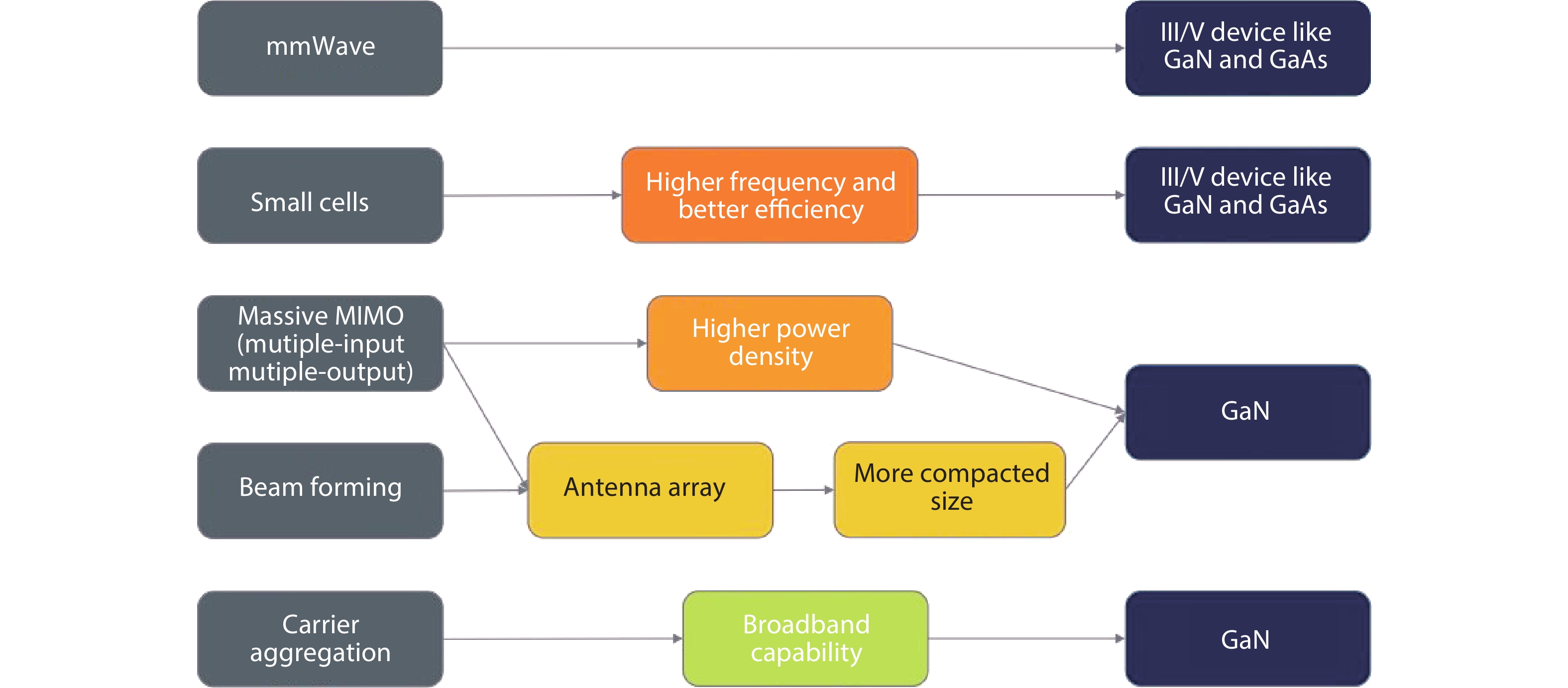
    (Color online) The main requirements in 5G wireless communication[4].
    Fig. 1. (Color online) The main requirements in 5G wireless communication[4].
    (Color online) GaN HEMTs for power electronics applications[8].
    Fig. 2. (Color online) GaN HEMTs for power electronics applications[8].
    (Color online) The routine failure analysis procedure for GaN HEMTs.
    Fig. 3. (Color online) The routine failure analysis procedure for GaN HEMTs.
    (Color online) (a) Schematic GaN HEMT cross section. (b) SEM image depicting damages after the catastrophic failure[22].
    Fig. 4. (Color online) (a) Schematic GaN HEMT cross section. (b) SEM image depicting damages after the catastrophic failure[22].
    (Color online) SEM and TEM images revealing different types of failure mechanisms dominant during test under (a) dark and (c) UV conditions. (b) TCAD contour revealing hole distribution at breakdown voltage, under the –6 V gate bias condition[24].
    Fig. 5. (Color online) SEM and TEM images revealing different types of failure mechanisms dominant during test under (a) dark and (c) UV conditions. (b) TCAD contour revealing hole distribution at breakdown voltage, under the –6 V gate bias condition[24].
    (Color online) A sequence of events captured during 50 ns ESD stresses on the drain without gate and with mesa[25].
    Fig. 6. (Color online) A sequence of events captured during 50 ns ESD stresses on the drain without gate and with mesa[25].
    (Color online) (a, c, e) SEM images and (b, d, f) AFM images of three devices with different stressed times[16].
    Fig. 7. (Color online) (a, c, e) SEM images and (b, d, f) AFM images of three devices with different stressed times[16].
    (Color online) (a) EMMI images of the device at different stress times. (b, c) TEM image of the failure region depicted in (a)[30].
    Fig. 8. (Color online) (a) EMMI images of the device at different stress times. (b, c) TEM image of the failure region depicted in (a)[30].
    (Color online) (a, b) EMMI images of the HEMT before and after ON-state DC-stress. (c, d) Cross-section EDS mapping of central T-gate finger showing the formation of Ni voids. (e) Aluminium oxidation at a pit[31].
    Fig. 9. (Color online) (a, b) EMMI images of the HEMT before and after ON-state DC-stress. (c, d) Cross-section EDS mapping of central T-gate finger showing the formation of Ni voids. (e) Aluminium oxidation at a pit[31].
    (a) STEM of a TiN metal inclusion, which has penetrated the AlGaN layer. (b) A nanocrack extending from a TiN metal inclusion into the channel area[33].
    Fig. 10. (a) STEM of a TiN metal inclusion, which has penetrated the AlGaN layer. (b) A nanocrack extending from a TiN metal inclusion into the channel area[33].
    (a) A device before loading. (b) The device at the on-set of source-drain leakage. (c) A metal inclusion appears at the drain region. (d) The metal inclusion penetrates the GaN layer. (e) The metal inclusion reaches the GaN-SiC interface. (f) The substrate is completely damaged at last[19].
    Fig. 11. (a) A device before loading. (b) The device at the on-set of source-drain leakage. (c) A metal inclusion appears at the drain region. (d) The metal inclusion penetrates the GaN layer. (e) The metal inclusion reaches the GaN-SiC interface. (f) The substrate is completely damaged at last[19].
    (Color online) (a) De-cap and de-layer operations of the failed device. (b) Simulation of electric field and impact ionization (I.I.) rate distributions along the AlGaN/GaN interface when the Vds approaches Vpeak during the UIS process[36].
    Fig. 12. (Color online) (a) De-cap and de-layer operations of the failed device. (b) Simulation of electric field and impact ionization (I.I.) rate distributions along the AlGaN/GaN interface when the Vds approaches Vpeak during the UIS process[36].
    (Color online) (a) TEM image and (b) EDS cartography (across the blue line) of the Schottky contact of an aged HEMT[37].
    Fig. 13. (Color online) (a) TEM image and (b) EDS cartography (across the blue line) of the Schottky contact of an aged HEMT[37].
    (Color online) (a) Burn spot locations for 50 W-pulses. (b) Simulated densities of power dissipation for two different pulses shortly before the failure happens. (c) A failure region (Mag = 500×)[38].
    Fig. 14. (Color online) (a) Burn spot locations for 50 W-pulses. (b) Simulated densities of power dissipation for two different pulses shortly before the failure happens. (c) A failure region (Mag = 500×)[38].
    (Color online) (a) Failure region of the GaN HEMT (CGH-27015, manufactured by Cree, Inc.). (b) FIB image of the breakdown area which is located in the FP. (c) Captured thermal stress distribution of the device. (d) Enlarged stress distribution near the gate[43].
    Fig. 15. (Color online) (a) Failure region of the GaN HEMT (CGH-27015, manufactured by Cree, Inc.). (b) FIB image of the breakdown area which is located in the FP. (c) Captured thermal stress distribution of the device. (d) Enlarged stress distribution near the gate[43].
    (Color online) (a) Optical image of the GaN HEMT before failure. (b) SEM image of the GaN HEMT after failure[46].
    Fig. 16. (Color online) (a) Optical image of the GaN HEMT before failure. (b) SEM image of the GaN HEMT after failure[46].
    (Color online) (a) Magnetic field distribution and (b) optical micrograph of the PA layout[46].
    Fig. 17. (Color online) (a) Magnetic field distribution and (b) optical micrograph of the PA layout[46].
    TEM images of GaN HEMT device irradiated with 1540 MeV Bi ions at a fluence of 1.7 × 10¹¹ ions/cm2[48]. (a) Cross-section of the gate areas. (b) High-resolution image of the tracks in heterogeneous junction areas as marked in (a). (c) High-resolution image of the tracks at a depth of about 500 nm as marked in (a). (d) Tracks formed in the drain area. (e) Tracks appearing at a depth of about 500 nm as marked in (d).
    Fig. 18. TEM images of GaN HEMT device irradiated with 1540 MeV Bi ions at a fluence of 1.7 × 10¹¹ ions/cm2[48]. (a) Cross-section of the gate areas. (b) High-resolution image of the tracks in heterogeneous junction areas as marked in (a). (c) High-resolution image of the tracks at a depth of about 500 nm as marked in (a). (d) Tracks formed in the drain area. (e) Tracks appearing at a depth of about 500 nm as marked in (d).
    TEM images at different VD during the OFF-state failure tests after the irradiation (2.8 MeV Au4+ ion species for 60 min to a fluence of 4 × 10¹⁴ ions/cm2)[49]. Drain voltage: (a) Vd = 0 V, (b) Vd = 10.2 V, and (c) enlarged TEM image of the yellow rectangle area of (b), showing dislocations in the GaN layer.
    Fig. 19. TEM images at different VD during the OFF-state failure tests after the irradiation (2.8 MeV Au4+ ion species for 60 min to a fluence of 4 × 10¹⁴ ions/cm2)[49]. Drain voltage: (a) Vd = 0 V, (b) Vd = 10.2 V, and (c) enlarged TEM image of the yellow rectangle area of (b), showing dislocations in the GaN layer.
    Failure typeFailure mechanismFailure phenomenaRef.
    ESDSelf-heatingMigration of S/D metal from D to S[23, 27, 28]
    Premature breakdown of parasitic SBDGate finger melts and migrates to S/D pads
    Inverse piezoelectric effectCrack in the G–D region
    Trap assisted hole injectionCrack in the S–G region, which extend to buffer layer[24, 27, 28]
    G–D electric field induced thermal stressCrack propagate from G to D
    Dislocation assisted current leakageGate finger peels off[28]
    Electric stress induced defect generationCrack and metal migration in the G–D region[25]
    High electric stressElectrochemical reaction with waterPits, groove and trench along drain-side gate[16, 29]
    Passivation layer (SiNx) breakdown Short-circuit path between gate edge and 2DEG[30]
    Gate contact degradationMetal migration at pads/AlGaN interface, crack[3133]
    Inverse piezoelectric effectBurning around drain contact[36]
    Dislocation assisted leakage currentDrain metal melt and penetrate to substrate[19]
    High thermal stressGate contact degradationRimous metal surface, migration of Au into Ni-semiconductor Schottky contact[37]
    Self-heatingBurn marks in the G–D region[38]
    Thermal expansion of FP metalCrack in FP[43]
    High magnetic fieldCombined effect of the operating current density and the eddy currentCrack and small granule in the G–D region, liquid gate metal propagates into underlying layer[46]
    Irradiation effectIrradiation damageLatent track, vacancy and dislocation[4749]
    Gate injectionEpitaxial layer peels off from substrate[49]
    Table 1. Different failure mechanisms and their corresponding failure phenomena.
    Xiaolong Cai, Chenglin Du, Zixuan Sun, Ran Ye, Haijun Liu, Yu Zhang, Xiangyang Duan, Hai Lu. Recent progress of physical failure analysis of GaN HEMTs[J]. Journal of Semiconductors, 2021, 42(5): 051801
    Download Citation