• Journal of Semiconductors
  • Vol. 42, Issue 5, 051801 (2021)
Xiaolong Cai1、2、3, Chenglin Du2、3, Zixuan Sun2、3, Ran Ye2、3, Haijun Liu2, Yu Zhang2, Xiangyang Duan2, and Hai Lu1
Author Affiliations
  • 1School of Electronic Science and Engineering, Nanjing University, Nanjing 210093 China
  • 2Architecture Team, Wireless Product Planning Department, ZTE Corporation, Nanjing 210012, China
  • 3State Key Laboratory of Mobile Network and Mobile Multimedia Technology, Shenzhen 518057, China
  • show less
    DOI: 10.1088/1674-4926/42/5/051801 Cite this Article
    Xiaolong Cai, Chenglin Du, Zixuan Sun, Ran Ye, Haijun Liu, Yu Zhang, Xiangyang Duan, Hai Lu. Recent progress of physical failure analysis of GaN HEMTs[J]. Journal of Semiconductors, 2021, 42(5): 051801 Copy Citation Text show less

    Abstract

    Gallium nitride (GaN)-based high-electron mobility transistors (HEMTs) are widely used in high power and high frequency application fields, due to the outstanding physical and chemical properties of the GaN material. However, GaN HEMTs suffer from degradations and even failures during practical applications, making physical analyses of post-failure devices extremely significant for reliability improvements and further device optimizations. In this paper, common physical characterization techniques for post failure analyses are introduced, several failure mechanisms and corresponding failure phenomena are reviewed and summarized, and finally device optimization methods are discussed.

    1. Introduction

    Thanks to the remarkable developments in wide-bandgap semiconductor technologies over the past few decades, gallium nitride (GaN)-based high-electron mobility transistors (HEMTs) have shown prominent performances in high power and high frequency application fields. The high charge density of the two-dimensional electron gas (2DEG) and the wide bandgap (~3.4 eV) of GaN result in the low resistance and the high-power density of GaN HEMTs. The high saturation electron velocity raises the switching frequency of GaN RF systems, and lowers their power loss and physical size. Moreover, when combined with silicon carbide (SiC) substrates, the low intrinsic carrier concentration of GaN and the high thermal conductivity of SiC offer a higher operating temperature, which insures operation under extreme environment conditions; on the other hand, the high maturity and the high integration level of Si substrates provide cost-effective Si-based GaN HEMTs[1-3].

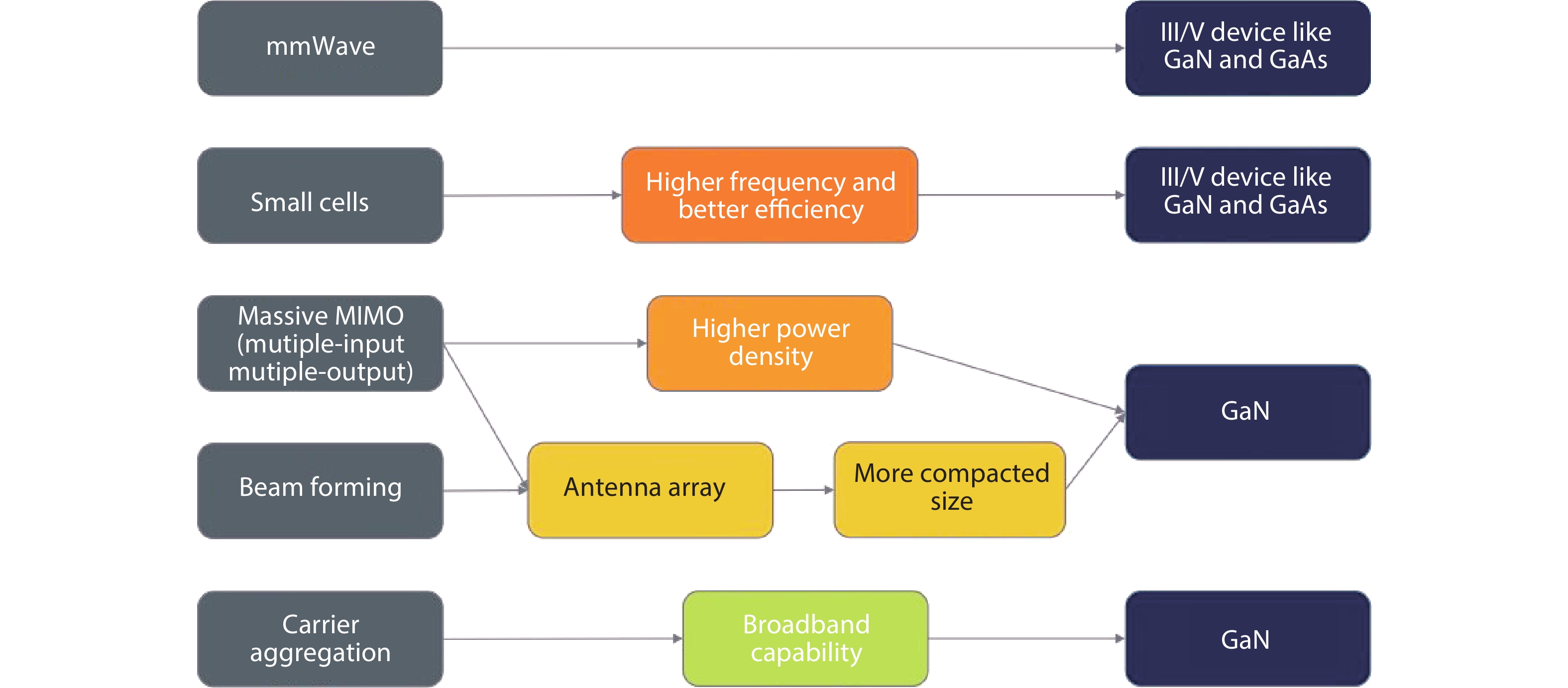
    Benefiting from all the excellent physical and chemical properties mentioned above, GaN HEMTs perfectly match the main requirements of devices for the fifth generation (5G) wireless communication (shown in Fig. 1) and power electronics, thus accelerating the growth of numerous applications (shown in Fig. 2), including millimeter-wave power amplifiers (PAs)[1], low noise amplifiers[2], threshold switching devices[3], battery chargers[5], power converters[6], and satellite communications[7], to name a few.

    (Color online) The main requirements in 5G wireless communication[4].

    Figure 1.(Color online) The main requirements in 5G wireless communication[4].

    (Color online) GaN HEMTs for power electronics applications[8].

    Figure 2.(Color online) GaN HEMTs for power electronics applications[8].

    However, GaN HEMTs can be influenced by various degradation mechanisms, which are not observed in Si or GaAs devices, due to operating conditions under larger current densities, higher temperatures and electric fields. Material properties, such as piezoelectric effects, heteroepitaxy on SiC or Si substrates, higher densities of deep-level defects and thermal interfaces with substrates and packages, could lead GaN HEMTs to degradations and even catastrophic failures[9]. Most of the degradation-related effects could be traced, measured and analyzed by electrical performance testing. Nevertheless, compared with the continuous degradation processes, catastrophic failures are instantaneous and hard to be analyzed by common electrical measurements. For this reason, more attention is drawn by long-term reliability and performance instability[10] research instead of physical analyses of post failures that are significant in reliability improvements of GaN HEMTs.

    Over these years, a few studies have focused on physical failure analyses of GaN HEMTs, and several failure mechanisms have been reported. In this paper, common physical characterization techniques for post-failure analyses are introduced, several failure mechanisms and corresponding failure phenomena are reviewed and summarized, and finally device optimization methods are discussed.

    2. Post-failure analysis procedure

    It is hard to find out where and how the failures begin on failed devices, since they have suffered catastrophic failures, and thus common electrical measurements are basically no longer effective. Therefore, emission microscope (EMMI), scanning electron microscope (SEM), focused ion beam (FIB), atomic force microscope (AFM), energy dispersive spectrometer (EDS), high resolution transmission electron microscope (TEM) and the technology computer-aided design (TCAD) simulation are the choices for post-failure analyses. The routine failure analysis procedure can be described as follows: firstly, failure zones are located by EMMI under a proper operating voltage and integral time; secondly, failure zones are dissected by FIB; thirdly, the cross-section of failure zones are observed by SEM, AFM and TEM, followed by the element analyses via EDS; and lastly, TCAD simulations are used to find out the failure reason, as shown in Fig. 3.

    (Color online) The routine failure analysis procedure for GaN HEMTs.

    Figure 3.(Color online) The routine failure analysis procedure for GaN HEMTs.

    2.1. EMMI

    In an EMMI system, a microscope is used to obtain the optically reflected image of the device under a white light illumination. The failure zone emits photons when there are current leakages, electric field crowdings, dislocations, or meltdown pits. The emitted photons are collected and converted into electrical signals by photoelectric detectors such as charge-coupled devices (CCDs) or photomultipliers. At last, an electroluminescence (EL) image of the device is formed, and the position of the failure zone can be located by superimposing an EL image on a reflected image. In the post-failure analyses of GaN HEMTs, based on a probe station system and bare devices, it is possible for an EMMI to detect the EL pattern of the device under different operating conditions. As a consequence, failure mechanisms can be analyzed through the intensities, the spatial distributions and the spectral characteristics of hot spots in the EL images and their evolutions over time[11, 12].

    2.2. FIB

    In an FIB system, the ion source produces a stable ion beam, which can be modulated by the focusing and scanning modules by controlling the size and the intensity of beam spot. The specimen station is applied to change the processing position. The SEM is not able to obtain the inner information of failed devices unless the FIB is utilized. With the assistance of FIB, failed devices can be dissected, and key information like the AlGaN/GaN interface, gate meltdown situations and dislocation paths can be acquired.

    2.3. SEM, TEM, and AFM

    In an SEM system, an electron beam emitted from the electron source gets accelerated and focused by magnetic fields and several magnetic lenses, and finally the incident beam beats down on the surface of the failed device specimen. With the help of the final lens (objective lens), which are equipped with axially-symmetric scan coils, the incident electron beam is able to accomplish the scans of the specimen. Once high-energy electrons enter the specimen, they can be scattered both elastically and inelastically, thus generating various signals including secondary electrons, backscattered electrons, transmitted electrons, etc[13]. The generated analog signals are received by corresponding detectors and translated into electrical signals. The electrical signals get amplified and converted into image signals, providing detailed information of failed devices, such as dislocation pits, cracks and the surface topographies of gate metal contacts.

    Compared with SEM, TEM retrieves information brought by transmitted electrons, meaning that the required accelerating voltage is higher and the specimen has to be thinner. It is able to obtain magnified images of FIB-thinned HEMT specimens (thickness ~10 nm), commonly with a magnification power in the range 103–106[14]. Moreover, TEM is capable of providing electron diffraction patterns, which are of use to analyze crystalline specimens[15].

    AFM is commonly used to conduct quantitative analyses and obtain scanned images of surface topographies of failed devices at a nanometer scale, especially at gate-edge regions. Before AFM scans, wet etches should be done to handle passivation layers and metal contacts. Normally, the hydrofluoric acid is utilized to remove passivation layers while metal contacts are targets for the aqua regia. Finally, the piranha solution is utilized for a short time to clean the entire organic contaminants and offers a pure surface for the following analyses[16].

    2.4. EDS

    X-ray is released when high-energy electrons react with specimens. As each element has its own X-ray characteristic energy, qualitative and quantitative component analyses of failure zones can be realized by using EDS. The combination of TEM and EDS is normally utilized to study the inner structure of failure zones such as channel layers, gate metal contacts, and buffer layers[17-21], etc. Details of the structure and the chemical contrast are observable at a nanometer scale.

    2.5. TCAD Simulation

    In the failure analysis, the TCAD simulations are commonly used to figure out the failure reason due to the low time consumption and analysis costs. Generally, the device structures are firstly built up by the TCAD simulators according to the real process. After that, the stress conditions applied on the devices are determined to reproduce the suffered failure process in the simulators. Finally, taking all the obtained results into consideration, the simulated inner states of the devices are analyzed and discussed to find out the physical failure mechanism. In this way, it is helpful for designers to determine the failure reason accurately and conveniently by using TCAD simulations.

    3. Failure mechanism analysis

    3.1. Electrostatic discharge (ESD)

    In 2015, Rossetto et al.[22] reported an analysis of GaN-on-Si HEMTs ESD robustness via drain-to-source transmission line pulse (TLP) stresses. The TLP IV curves tested under varying VG levels prove that the failure is owing to a power-dependent process under ON-state; when OFF-state is considered, the device fails due to a field-dependent mechanism. Under high power dissipation conditions during ON-state, small dark spots can be seen in SEM images; under OFF-state at a higher degradation voltage and a lower VG, large dark spots and cracks are the main failure phenomena, as shown in Fig. 4(b).

    (Color online) (a) Schematic GaN HEMT cross section. (b) SEM image depicting damages after the catastrophic failure[22].

    Figure 4.(Color online) (a) Schematic GaN HEMT cross section. (b) SEM image depicting damages after the catastrophic failure[22].

    In 2016, Shankar et al.[23] reported three failure mechanisms of GaN HEMTs under ESD stress conditions: (a) Devices without mesa isolations and gate contacts fail owing to the migrations of metal contacts from the drain to the source. Metal migrations at the contact corners are remarkable, due to the existence of the largest field crowding there. Under higher ESD currents, the temperature of device lattices is sufficient to melt the metal pads. The liquid metal flows across the S–D region under the fringing electric field, thus creating an electrical short. (b) The premature breakdown of the parasitic Schottky barrier diode (SBD) between the gate track and the mesa edge is also a root failure mechanism for ESD cases. The melted gate metal damages the gate finger, and creates a short between pads of the source and the drain. (c) Devices stressed under the grounded gate utilizing short TLP (pulse width < 10 ns) exhibits several cracks between the drain and the gate finger. The pulse width is too short for the drain current to accomplish snapbacks, most of the energy remains in devices, hence the inverse piezoelectric effect induced by the high electric field leads to the final damages.

    In 2017, Shankar et al.[24] reported a research of the physical mechanisms of the safe operating area (SOA) and the avalanche instability in GaN HEMTs utilizing a sub-μs pulse characterization. Fig. 5(a) shows the observed damage marks in the S–G area of the HEMT, which fails under a dark condition, the TEM cross section image along line ‘a–b’ reveals several cracks that have penetrated down to the buffer layer. The failure is owing to hole accumulations around the gate region and the formation of localized parasitic/filament paths. TCAD simulations demonstrate that a higher density of surface traps enhance the electric field at the gate edge (both at the surface and inside the channel), while a higher density of buffer traps enhance the electric field under the drain contacts, as shown in Fig. 5(b). Due to the impact ionization, excess holes generate at the drain-edge region and inject into the buffer layer. They are collected near the source, then the parasitic S–G short paths are formed. Fig. 5(c) shows the damages in the G–D region of the HEMT which fails under an UV illumination condition (stressed using 10 ns pulses). SEM images taken along line ‘A–B’ reveals cracks under the drain-side gate edge, which have extended to the source. The electric field peaks at the drain-side gate edge in absence of traps (in the presence of UV light), it generates a thermal stress near the gate and triggers crack formations. Under the G–D electric stress, the cracks extend to the drain.

    (Color online) SEM and TEM images revealing different types of failure mechanisms dominant during test under (a) dark and (c) UV conditions. (b) TCAD contour revealing hole distribution at breakdown voltage, under the –6 V gate bias condition[24].

    Figure 5.(Color online) SEM and TEM images revealing different types of failure mechanisms dominant during test under (a) dark and (c) UV conditions. (b) TCAD contour revealing hole distribution at breakdown voltage, under the –6 V gate bias condition[24].

    In the same year, an on-the-fly monitoring of the device was carried out to investigate the evolution of device failures, utilizing a high-resolution optical microscope system and a high-speed integrated CCD camera. Shankar et al. reported that repeated stresses (increase in number with a fixed amplitude) give rise to the accumulative degradations and the early device failure. This cumulative character of degradations is owing to the defect generation and the carrier trapping in various regions of the device. Fig. 6 shows the device under stresses at different moments of time[25].

    (Color online) A sequence of events captured during 50 ns ESD stresses on the drain without gate and with mesa[25].

    Figure 6.(Color online) A sequence of events captured during 50 ns ESD stresses on the drain without gate and with mesa[25].

    In 2019, Canato et al.[26] investigated the ESD robustness of E-mode devices. It is demonstrated that the failure under the ON-state is attributed to a current-dependent process and the failure appears at random positions along the gate finger, and no obvious hot spots can be seen. The failures happen under random power dissipation conditions, indicating that the power-related issue is beyond the major mechanism. On the other hand, the failure voltage Vd drops as VG increases, hence the drain current is considered to play the main role in the failure mechanism.

    In the same year, Shankar et al.[27] reported the influence of self-heating, carrier trapping and piezoelectric field on GaN HEMT ESD failures: (a) Under large electric field, carriers become hot and then transfer their energy to lattices, thus generating acoustic and optical phonons. With picosecond-level lifetime and low group velocity, optical phonons in GaN accumulate and form hotspots, finally giving rise to local self-heating and catastrophic failures. (b) At larger ESD pulse widths, the trapping occurs for the longer duration. The risen lattice temperature facilitates thermal excitation of valence electrons to defect levels, thus leaving holes behind in buffer layers. The potential holes accumulate in the buffer, which cause avalanche breakdowns and then device failures. (c) The normal component of the channel electric field, which distributes along the [0001] direction, introduces in-plane biaxial tensile stress in GaN/AlGaN layers due to the inverse piezoelectric effect. Once the stored elastic energy reaches its critical value under strong field or high temperature, it releases and forms crystallographic defects.

    In 2020, Shankar et al.[28] reported the role of surface passivation, mesa isolation and threaded dislocation in defining the failure type of GaN HEMTs under ESD stress conditions: (a) The ESD failure seems independent of the surface passivation condition in the case. The inverse piezoelectric effect explains the failure better and the surface conditions are observed to have minimal influence on the ESD robustness of devices. (b) For the HMET without mesa isolation, the fringing field facilitates crack formations and metal migration, and leads to early failure at corners. (c) Threaded dislocations near the gate provide paths for the metal diffusion, which triggers the local Schottky junction degradation and causes the gate leakage increment. The gate finger is weakened by all the factors and finally peels off at the dislocation site under the increasing TLP stress.

    3.2. High electric stress

    In 2015, Wu et al.[16] reported a direct relation between structural and electrical degradations of GaN HEMTs under high-power and high-temperature direct current stresses. Under high electric stresses, the IDmax degrades with stress time due to the structural deformation, as shown in Fig. 7. Shallow grooves appear along the drain-side gate metal fingers in the HEMTs with a mild IDmax degradation. Deep pits are formed in the HEMTs with an obvious IDmax degradation. As the drain current degradation rises from 0.2% to 25.8%, gate-edge damages develop from shallow grooves into distinct ravines which are deep enough to pierce through the buffer region and cause the final catastrophic failure.

    (Color online) (a, c, e) SEM images and (b, d, f) AFM images of three devices with different stressed times[16].

    Figure 7.(Color online) (a, c, e) SEM images and (b, d, f) AFM images of three devices with different stressed times[16].

    A possible reason for the structural deformation underneath the gate region is electrochemical reactions between water and AlGaN[29]. The utilized HEMTs are not in hermetic packages, hence water vapour may creep in and contribute to the observed phenomena. The redox reaction between the AlGaN layer and water can be described by the formula as follows:

    $ 2{\rm{A}}{{\rm{l}}_x}{\rm{G}}{{\rm{a}}_1}_{-x}{\rm{N}} + 3{{\rm{H}}_2}{\rm{O}} = x{\rm{A}}{{\rm{l}}_2}{{\rm{O}}_3} + (1-x){\rm{G}}{{\rm{a}}_2}{{\rm{O}}_3} + {{\rm{N}}_2} \uparrow +\, 3{{\rm{H}}_2} \uparrow . $  (1)

    In 2016, Rossetto et al.[30] demonstrated that the drain-side gate edge of GaN HEMTs under high electric stress is a weakness, where the electric field crowding in the passivation layer approaches the critical value of SiNx. They proved that the catastrophic failure is attributed to the formation of a short-circuit path between the gate-foot edge and the 2DEG in the drain-side. Small hot spots are detected in the EMMI system and their intensity rises as the stress time increases; a red spot can be clearly observed just before the catastrophic failure occurs, as shown in Fig. 8(a). The TEM images presents a path connecting the SiNx layer and the AlGaN layer, as shown in Figs. 8(b) and 8(c).

    (Color online) (a) EMMI images of the device at different stress times. (b, c) TEM image of the failure region depicted in (a)[30].

    Figure 8.(Color online) (a) EMMI images of the device at different stress times. (b, c) TEM image of the failure region depicted in (a)[30].

    In 2017, the influence of gate metallizations on the reliability of SiC-based GaN HEMTs were investigated by Dammann et al.[31]. Ni voids and pits depicted by EMMI and TEM images near the gate-foot are regarded as the major failure reason of HEMTs with NiPtAu T-gates. Stressed devices are mapped by a high-resolution EDS system, where it is found that a local aluminium oxidation procedure leads to the formation of pits, as shown in Fig. 9. The interface between the AlGaN layer and the negatively charged pits is in the vicinity of the channel and, as a consequence, the conduction band slope and lateral electrical field near the gate-foot increases. This might cause a higher electric stress and trigger deformations at the location of the pit. Sin et al.[32] conducted similar tests on RF GaN HEMTs, and their results demonstrate that Pd-enriched pits/defects can also form at the interface between the AlGaN layer and the spacer-gate-edge.

    (Color online) (a, b) EMMI images of the HEMT before and after ON-state DC-stress. (c, d) Cross-section EDS mapping of central T-gate finger showing the formation of Ni voids. (e) Aluminium oxidation at a pit[31].

    Figure 9.(Color online) (a, b) EMMI images of the HEMT before and after ON-state DC-stress. (c, d) Cross-section EDS mapping of central T-gate finger showing the formation of Ni voids. (e) Aluminium oxidation at a pit[31].

    In the same year, Whiting et al.[33] reported the formation of nanocracks underneath the ohmic metal contacts of GaN HEMTs. Wet etches are done to remove the ohmic contacts of electrically stressed devices, and it is found that the observed nanocracks orient along the [11-20] directions. Normally, metal inclusions are formed underneath the contacts during the rapid thermal annealing (RTA) process, as shown in Fig. 10(a). Analysis data suggests that the cracks might grow from the metal inclusions under the influence of a vertically-oriented electric field which introduces a biaxial stress in the channel layer. The hoop stresses introduced by the biaxial compressive stresses and the residual tensile stress introduced in the epitaxial process impel the cracks to extend from the alloyed S–D contacts into the channel, as shown in Fig. 10(b). In 2018, Mazumdar et al. reported that the inverse piezoelectric effect in GaN HEMTs may also cause the formation of nanocracks, and the formation process can be described by Griffith’s theory of brittle fracture[34]. When an electric stress is applied on a GaN HEMT, the inverse piezoelectric effect occurs and extra mechanical stresses are introduced into the epilayer. Once the accumulated elastic energy reaches the limit of the epilayer, the excessive mechanical stresses release through the formation of crystallographic cracks[35].

    (a) STEM of a TiN metal inclusion, which has penetrated the AlGaN layer. (b) A nanocrack extending from a TiN metal inclusion into the channel area[33].

    Figure 10.(a) STEM of a TiN metal inclusion, which has penetrated the AlGaN layer. (b) A nanocrack extending from a TiN metal inclusion into the channel area[33].

    In 2018, Islam et al.[19] reported the real-time visualization of GaN HEMT failures by operating the devices inside a TEM. The in-situ TEM technique can characterize the lattice dislocations and metal diffusion and thus monitor the degradation of the epilayer quality during the whole failure process. Fig. 11(a) reveals a network of pre-existing dislocations which facilitate local charge accumulations and lower the breakdown strength, and catastrophic failures may occur through the dislocation percolation. As VD increases, ID becomes large enough to activate the dislocations (marked by arrows 2 and 3) that have moved towards the gate region, as shown in Fig. 11(b). The dislocation transformation leads to very large leakage current density, causing damages at the drain metal contacts and the subsequent epilayer and substrate, as shown in Figs. 11(c)11(f). At first, a metal inclusion forms under the drain region (marked by arrow t1), which penetrates the GaN layer about 6.2 s later. It then takes less than a second to reach the GaN-substrate interface and finally the substrate is completely damaged by the metal diffusion. The presented “seeing while measuring” in-situ TEM technique can be effective in finding out the dominant failure mechanisms and their fundamental origins.

    (a) A device before loading. (b) The device at the on-set of source-drain leakage. (c) A metal inclusion appears at the drain region. (d) The metal inclusion penetrates the GaN layer. (e) The metal inclusion reaches the GaN-SiC interface. (f) The substrate is completely damaged at last[19].

    Figure 11.(a) A device before loading. (b) The device at the on-set of source-drain leakage. (c) A metal inclusion appears at the drain region. (d) The metal inclusion penetrates the GaN layer. (e) The metal inclusion reaches the GaN-SiC interface. (f) The substrate is completely damaged at last[19].

    In 2020, Liu et al.[36] firstly reported the single pulse unclamped inductive switching (UIS) withstanding physics and failure mechanism for p-GaN HEMT. All evidence eliminates other failure mechanisms, leaving the inverse piezoelectric effect to be the predominant one. De-cap and de-layer operations are carried out to verify the failure mechanisms, which indicates that the most serious burning locates at the drain contact, as shown in Fig. 12(a). Combining the TCAD simulation data shown in Fig. 12(b), it can be concluded that the inverse-piezoelectric effect might occur near the drain when the electric field is very strong. It induces dislocations and causes a sharp increment of the leakage current. Consequently, the hot regions near drain contacts are burned by thermal runaway. Furthermore, it is proved that larger bus voltage and load inductance grow the failure risk induced by UIS stress, while the gate resistance, turn-OFF gate voltage and ambient temperature have little impacts upon the UIS capability of the p-GaN HEMT.

    (Color online) (a) De-cap and de-layer operations of the failed device. (b) Simulation of electric field and impact ionization (I.I.) rate distributions along the AlGaN/GaN interface when the Vds approaches Vpeak during the UIS process[36].

    Figure 12.(Color online) (a) De-cap and de-layer operations of the failed device. (b) Simulation of electric field and impact ionization (I.I.) rate distributions along the AlGaN/GaN interface when the Vds approaches Vpeak during the UIS process[36].

    3.3. High thermal stress

    In 2016, Temcamani et al.[37] investigated failure mechanisms of Si-based GaN HEMT RF PAs under radar operating conditions. Characterizations performed before and after ageing tests prove that gate metal contacts are very sensitive to temperatures, and the irreversible part of the ageing process at gate region is mainly due to thermal stresses. During the ageing tests, pristine HEMTs are aged in a thermally regulated oven at 250 °C for 200 h, and then at 300 °C for 200 h again. The surfaces of metallic zones appear strongly and densely crackled, meanwhile EDS measurements confirm an Au inclusion between the Ni layer and the AlGaN layer, as shown in Fig. 13.

    (Color online) (a) TEM image and (b) EDS cartography (across the blue line) of the Schottky contact of an aged HEMT[37].

    Figure 13.(Color online) (a) TEM image and (b) EDS cartography (across the blue line) of the Schottky contact of an aged HEMT[37].

    In 2017, Mocanu et al.[38] reported the predominant defect mechanism and the electrothermal stability of Schottky-gate GaN HEMTs. A DC module, which measures the device performance up to a temperature as high as 400 °C, is developed to ascertain the SOA thermal limitations of devices, and tests up to failure are applied at different operating sites[39]. The main failure reason is confirmed to be the formation of hot spots and the following thermal runaway. The thermal runaway is due to a heavy drain-gate leakage current which occurs under elevated temperature stresses. The observed burn spots distribute along the gate metal fingers, as shown in Fig. 14(a). The temperature distributions along Schottky contacts of gates are considered to be non-uniform, owing to the tunneling current induced by local defects[40] or the Schottky barrier height inhomogeneities[41]. At high-temperature (T > 400 °C) regions, leakage currents sharply rises with T, thus resulting in self-heating spots[42]. Fig. 14(b) shows the electrothermal simulation of power dissipation densities shortly before failure. The power dissipation is more non-uniform for 400 V than for 50 V, indicating the earlier start of the hot spot formation. As the hot spots appear, the device approaches a higher temperature, and the leakage currents between the drain and the gate give rise to an excess power dissipation, finally causing the thermal runaway and the catastrophic failure, as shown in Fig. 14(c).

    (Color online) (a) Burn spot locations for 50 W-pulses. (b) Simulated densities of power dissipation for two different pulses shortly before the failure happens. (c) A failure region (Mag = 500×)[38].

    Figure 14.(Color online) (a) Burn spot locations for 50 W-pulses. (b) Simulated densities of power dissipation for two different pulses shortly before the failure happens. (c) A failure region (Mag = 500×)[38].

    In the same year, Zhou et al.[43] studied the thermal stress breakdown of GaN HEMTs under large microwave injected pulses. A burn mark is clearly seen in the failure region of the device, as shown in Fig. 15(a). The FIB cross section image [Fig. 15(b)] displays a crack in the field plate (FP). SiNx passivation layers are applied on the Au-made gate and its FP in order to decrease the current collapse of devices. According to the proposed thermal breakdown model and corresponding simulation results, the stress peak is located at the gate edge and the FP. The stress peak is lower than the critical yield strength of SiNx (2400 MPa), while the stress in the FP is larger than that of Au (200 MPa)[44, 45]. The FP with a large thermal expansion coefficient is greatly affected by the thermal stress, and therefore, the cracks start from the FP.

    (Color online) (a) Failure region of the GaN HEMT (CGH-27015, manufactured by Cree, Inc.). (b) FIB image of the breakdown area which is located in the FP. (c) Captured thermal stress distribution of the device. (d) Enlarged stress distribution near the gate[43].

    Figure 15.(Color online) (a) Failure region of the GaN HEMT (CGH-27015, manufactured by Cree, Inc.). (b) FIB image of the breakdown area which is located in the FP. (c) Captured thermal stress distribution of the device. (d) Enlarged stress distribution near the gate[43].

    3.4. High magnetic field

    In 2020, a new failure mechanism in the GaN HEMT PAs, which operate at high frequency and high power conditions, was reported by Sangwan et al.[46]. Metal electrodes of the drain and the gate melt down in the failed devices. Detailed analyses demonstrate that the eddy current triggered by the magnetic field from the nearby coil is one of the related failure mechanisms. On the other hand, the high operating current may also facilitate the failure process. An obvious cracked layer could be seen over the damaged drain and gate areas, as shown in Fig. 16. During the cooling down process of the melted metal (Au), small granules are formed in the failure region. The meltdown occurs at the Au layer and several hints of Au can be traced in either subsequent layer.

    (Color online) (a) Optical image of the GaN HEMT before failure. (b) SEM image of the GaN HEMT after failure[46].

    Figure 16.(Color online) (a) Optical image of the GaN HEMT before failure. (b) SEM image of the GaN HEMT after failure[46].

    The simulated magnetic field distribution over the integrated circuit is shown in Fig. 17(a), in which the peak magnetic field is near inductors. The large-inductance inductors, which carry highly amplified signals, are arranged in close vicinity to one other near the output port, giving rise to the high magnetic field strength during the circuit output stage. The magnetic field of the failure region is about 2.99 × 10² A/m, reaching the highest value among all the devices in the circuit. Once the total amount of the magnetic-induced eddy current and the operation current increase, remarkable Joule heatings in the drain and the gate metal regions occur and cause the observed failure of the device.

    (Color online) (a) Magnetic field distribution and (b) optical micrograph of the PA layout[46].

    Figure 17.(Color online) (a) Magnetic field distribution and (b) optical micrograph of the PA layout[46].

    3.5. Irradiation effect

    In 2018, Lei et al.[47] reported the degradation of GaN HEMTs, which were irradiated by 800 MeV Bi ions. As the fluence increases to 5.28 × 10¹⁰ ions/cm2, the saturation drain current reduces by 15% and the maximum transconductance decreases by more than 27%. A post physical analysis suggests that the degradation of device output performances is caused by ion-induced latent tracks.

    In the same year, Hu et al.[48] reported that the positive threshold voltage increases by about 85% due to the irradiation with 1540 MeV Bi ions at a fluence of 1.7 × 10¹¹ ions/cm2. The ion tracks penetrate the whole gate region and the heterogeneous junction, as shown in Fig. 18(a). The high-resolution images of tracks marked in Fig. 18(a) are shown in Figs. 18(b) and 18(c). The tracks through the whole epilayer in the HEMT is shown in Figs. 18(d) and 18(e). Further analyses indicate that the Bi-ions-irradiation-induced defects and disorders decrease the carrier density and mobility of 2DEG and finally lead to the degradation of the devices.

    TEM images of GaN HEMT device irradiated with 1540 MeV Bi ions at a fluence of 1.7 × 10¹¹ ions/cm2[48]. (a) Cross-section of the gate areas. (b) High-resolution image of the tracks in heterogeneous junction areas as marked in (a). (c) High-resolution image of the tracks at a depth of about 500 nm as marked in (a). (d) Tracks formed in the drain area. (e) Tracks appearing at a depth of about 500 nm as marked in (d).

    Figure 18.TEM images of GaN HEMT device irradiated with 1540 MeV Bi ions at a fluence of 1.7 × 10¹¹ ions/cm2[48]. (a) Cross-section of the gate areas. (b) High-resolution image of the tracks in heterogeneous junction areas as marked in (a). (c) High-resolution image of the tracks at a depth of about 500 nm as marked in (a). (d) Tracks formed in the drain area. (e) Tracks appearing at a depth of about 500 nm as marked in (d).

    In 2019, Islam et al.[49] proved that the heavy ion irradiation induces device damages by creating lattice defects, and accelerate degradations of the GaN HEMT under tests (CGHV1J006D, manufactured by Wolfspeed); on the other hand, a gate injection triggers impact ionization in the channel, thus inducing failures under the OFF-state. A HEMT just after the failure at VD = 10.2 V is shown in Fig. 19(b), its breakdown drain bias becomes lower compared with the pristine one, owing to the defect generations between the channel layer and the buffer layer during the ion irradiation. The generated defects accumulate local charges in the buffer layer, lower the breakdown strength and facilitate failures through their percolation. The drain edge of gate contacts suffer the largest electric field under the OFF-state, once ion irradiation prominently damages the gate Schottky contact, the gate injection sharply rises. The gate injection enhancement triggers the impact ionization in the channel, thus inducing the failure under the OFF-state.

    TEM images at different VD during the OFF-state failure tests after the irradiation (2.8 MeV Au4+ ion species for 60 min to a fluence of 4 × 10¹⁴ ions/cm2)[49]. Drain voltage: (a) Vd = 0 V, (b) Vd = 10.2 V, and (c) enlarged TEM image of the yellow rectangle area of (b), showing dislocations in the GaN layer.

    Figure 19.TEM images at different VD during the OFF-state failure tests after the irradiation (2.8 MeV Au4+ ion species for 60 min to a fluence of 4 × 10¹⁴ ions/cm2)[49]. Drain voltage: (a) Vd = 0 V, (b) Vd = 10.2 V, and (c) enlarged TEM image of the yellow rectangle area of (b), showing dislocations in the GaN layer.

    The failure mechanisms mentioned in Section 3 and their corresponding failure phenomena are summarized in Table 1.

    Table Infomation Is Not Enable

    4. GaN HEMTs optimization methods

    4.1. Surface passivation optimization

    GaN HEMTs with high-κ passivation layers are confirmed to achieve better breakdown performances and interface qualities[50, 51]. Since the high-κ material enhances the relative permittivity of the passivation layer εr, the electric field at the drain-side gate edge weakens, thus the breakdown voltage under the OFF-state improves. As the applied voltage in the insulator tends to descends uniformly, the voltage drops at the drain-side gate edge become smoother when the insulator is attached to the semiconductor. The higher the insulator εr, the better the optimization effect[52].

    On the other hand, in situ SiNx has advantages in improving defect levels and dielectric qualities when compared with ex situ SiNx. A near-ideal dielectric breakdown strength of ~13.2 MV/cm, a high interface quality with a state density of ~3.0 × 10¹² eV–1 cm–2 and a maximum forward bias as high as 19.5 V (~3.66 MV/cm) for a ten-year lifetime at the failure level of 0.01% are obtained by Cheng et al.[53]. The as-proposed in situ SiNx grown method offers an appropriate replacement for the passivation optimization, hence providing extra process facilitations and design adaptabilities.

    4.2. Gate recess depth and contact structure optimization

    By changing recess depths, the electric field in the channel layer and the buffer layer, which directly influences the SOA boundary in GaN HEMTs, can be tuned[54]. Devices without recess suffer about 30% degradation in VD, 15 nm recessed devices only degrades about 10%. It should be noted that the fully recessed devices undergo the maximum degradation (90%). For intermediate recess cases, the electric field crowdings are repressed since the field redistributes at gate or drain edges. The field repression at the drain decreases the impact ionization rate, thus avoiding premature avalanches in HEMTs. The lower field at the gate delays the formation of hot spots and the degradation induced by hot electrons. As a consequence, the redistribution of the channel field with the optimum recess depth improves the robustness and the SOA of devices.

    Schottky-type gate contacts are faced with gate stability problems, being easily affected by operation temperatures and the positive gate bias, especially in a low positive gate bias region. On the other hand, ohmic-type gate contacts exhibit a better stability against operation temperatures and the gate bias[55]. A combination of the two types of gate contact structures may lead to a balance between the gate stability and the control capability.

    4.3. Geometry optimization

    Rossetto et al.[22] demonstrated that as the FP length decreases, the catastrophic failure robustness dramatically improves since the FP edge is more far away from the ohmic contacts. An ESD robustness improvement about 40% is achieved if the FP length decreases from 5 to 1 µm, accordingly the failure voltage improves from 120 to 180 V for the optimized geometries under consideration.

    Fletcher et al.[56] proved that the discrete FP technique is useful to improve the RF and DC performance of GaN HEMTs. Compared with the conventional FP, it diminishes the peak of the electric field more effectively, and enhances the breakdown voltage from 298 to 330 V. Moreover, discrete-FP HEMTs significantly reduces the gate-source capacitance and gate-drain capacitance, which is important in high-frequency applications.

    4.4. GaN material quality optimization

    Since the device reliability and the GaN epitaxy are strongly correlated, high crystalline qualities and smooth surface morphology of the GaN epi-layers are extremely necessary. A remarkable enhancement in surface morphology of the GaN epi-structure along with better 2DEG properties and crystalline quality can be achieved by varying the V/III molar ratio[57, 58]. At a higher ratio, both point defects and carbon incorporation considerably decrease the GaN epi-layer, leading to a better device reliability.

    Wosko et al.[58] demonstrated the availability of in situ grown non-continous SiNx layers in the improvements of stress reduction and material epitaxy of GaN layers deposited on silicon substrates. The as-grown specimen with the SiNx nano-layer shows excellent structural properties, with GaN (0002) diffraction peak’s full width at half maximum of 362 arcsec and calculated basal plane stress lower than 200 MPa.

    The impurity doping, such as Mg[59] and carbon[60], during the initial growth of GaN buffer layers are found to compensate unintentional donors and reduce the defect density. Therefore, the device breakdown voltage and the material quality are enhanced by limiting the propagation of defects and dislocations.

    5. Conclusions

    In this review, common physical characterization techniques for the post failure analysis and the corresponding routine analysis procedure are introduced. Different types of failure mechanisms including ESD, high electric stress, high thermal stress, high magnetic field, irradiation effect, and the related failure mechanisms are reviewed. The failure phenomena corresponding to each failure mechanism are also summarized. Finally optimization methods for GaN HEMTs, such as surface passivation optimization, gate recess depth optimization, contact structure optimization and geometry optimization are discussed.

    Acknowledgements

    This work is supported by the National Key R&D Program of China (No. 2017YFB0403000).

    References

    [1] M H Mi, X H Ma, L Yang et al. Record combination fmax·Vbr of 25 THz·V in AlGaN/GaN HEMT with plasma treatment. AIP Adv, 9, 045212(2019).

    [2] D K Panda, G Amarnath, T R Lenka et al. Small-signal model parameter extraction of E-mode N-polar GaN MOS-HEMT using optimization algorithms and its comparison. J Semicond, 39, 64(2018).

    [3] X Huang, R Fang, C Yang et al. Steep-slope field-effect transistors with AlGaN/GaN HEMT and oxide-based threshold switching device. Nanotechnology, 30, 215201(2019).

    [4]

    [5] A Taylor, J Lu, L Zhu et al. Comparison of SiC MOSFET-based and GaN HEMT-based high-efficiency high-power-density 7.2 kW EV battery chargers. Power Electron, 11, 1849(2018).

    [6] R Faraji, H Farzanehfard, G Kampitsis et al. Fully soft-switched high step-up non-isolated three-port DC-DC converter using GaN HEMTs. IEEE Trans Ind Electron, 67, 8371(2020).

    [7] X Chen, W Zhai, J Zhang et al. FEM thermal analysis of high power GaN-on-diamond HEMTs. J Semicond, 39, 104005(2018).

    [8]

    [9]

    [10]

    [11] I Rossetto, M Meneghini, A Tajalli et al. Evidence of hot-electron effects during hard switching of AlGaN/GaN HEMTs. IEEE Trans Electron Devices, 64, 3734(2017).

    [12] M M Bajo, H Sun, M J Uren et al. Time evolution of off-state degradation of AlGaN/GaN high electron mobility transistors. Appl Phys Lett, 104, 223506(2014).

    [13] T Luo, A Khursheed. Elemental identification using transmitted and backscattered electrons in an SEM. Phys Procedia, 1, 155(2008).

    [14]

    [15] A Gkanatsiou, C B Lioutas, N Frangis et al. Influence of 4H-SiC substrate miscut on the epitaxy and microstructure of AlGaN/GaN heterostructures. Mat Sci Semicond Proc, 91, 159(2019).

    [16] Y Wu, C Y Chen, J A Del Alamo. Electrical and structural degradation of GaN high electron mobility transistors under high-power and high-temperature direct current stress. J Appl Phys, 117, 025707(2015).

    [17] B Wang, Z Islam, A Haque et al. In situ transmission electron microscopy of transistor operation and failure. Nanotechnology, 29, 31LT01(2018).

    [18] D Marcon, G Meneghesso, T L Wu et al. Reliability analysis of permanent degradations on AlGaN/GaN HEMTs. IEEE Trans Electron Devices, 60, 3132(2013).

    [19] Z Islam, A Haque, N Glavin. Real-time visualization of GaN/AlGaN high electron mobility transistor failure at off-state. Appl Phys Lett, 113, 183102(2018).

    [20] D D Wang, Y M Huang, P K Tan et al. Two planar polishing methods by using FIB technique: Toward ultimate top-down delayering for failure analysis. AIP Adv, 5, 127101(2015).

    [21] K Kumakura, T Makimoto. Growth of GaN on sapphire substrates using novel buffer layers of ECR-plasma-sputtered Al2O3/graded-AlON/AlN/Al2O3. J Cryst Growth, 292, 155(2006).

    [22] I Rossetto, M Meneghini, M Barbato et al. Demonstration of field- and power-dependent ESD failure in AlGaN/GaN RF HEMTs. IEEE Trans Electron Devices, 62, 2830(2015).

    [23]

    [24]

    [25]

    [26] E Canato, M Meneghini, A Nardo et al. ESD-failure of E-mode GaN HEMTs: Role of device geometry and charge trapping. Microelectron Reliab, 100/101, 113334(2019).

    [27] B Shankar, S Raghavan, M Shrivastava. ESD reliability of AlGaN/GaN HEMT technology. IEEE Trans Electron Devices, 66, 3756(2019).

    [28] B Shankar, S Raghavan, M Shrivastava. Distinct failure modes of AlGaN/GaN HEMTs under ESD conditions. IEEE Trans Electron Devices, 67, 1567(2020).

    [29] F Gao, S C Tan, J A Del Alamo et al. Impact of water-assisted electrochemical reactions on the off-state degradation of AlGaN/GaN HEMTs. IEEE Trans Electron Devices, 61, 437(2014).

    [30] I Rossetto, M Meneghini, S Pandey et al. Field-related failure of GaN-on-Si HEMTs: Dependence on device geometry and passivation. IEEE Trans Electron Devices, 64, 73(2017).

    [31] M Dammann, M Baeumler, V Polyakov et al. Reliability of 100 nm AlGaN/GaN HEMTs for mm-wave applications. Microelectron Reliab, 76/77, 292(2017).

    [32] Y Sin, D Veksler, J Bonsall et al. Electrical and structural characteristics of aged RF GaN HEMTs and irradiated high-power GaN HEMTs with protons and heavy ions. Gallium Nitride Materials and Devices XIV, 10918(2019).

    [33] P G Whiting, N G Rudawski, M R Holzworth et al. Nanocrack formation in AlGaN/GaN high electron mobility transistors utilizing Ti/Al/Ni/Au ohmic contacts. Microelectron Reliab, 70, 41(2017).

    [34] K Mazumdar, S Kala, A Ghosal et al. Nanocrack formation due to inverse piezoelectric effect in AlGaN/GaN HEMT. Superlattice Microst, 125, 120(2019).

    [35] Q Zhu, X Ma, B Hou et al. Investigation of inverse piezoelectric effect and trap effect in AlGaN/GaN HEMTs under reverse-bias step stress at cryogenic temperature. IEEE Access, 8, 35520(2020).

    [36] S Y Liu, S Li, C Zhang et al. Single pulse unclamped-inductive-switching induced failure and analysis for 650 V p-GaN HEMT. IEEE Trans Power Electr, 35, 11328(2020).

    [37] F Temcamani, J B Fonder, O Latry et al. Electrical and physical analysis of thermal degradations of AlGaN/GaN HEMT under radar-type operating life. IEEE Trans Microw Theory, 64, 756(2016).

    [38] M Mocanu, C Unger, M Pfost et al. Thermal stability and failure mechanism of Schottky gate AlGaN/GaN HEMTs. IEEE Trans Electron Devices, 64, 848(2017).

    [39]

    [40] R Jos. Reverse Schottky gate current in AlGaN-GaN high-electron-mobility-transistors. J Appl Phys, 112, 94508(2012).

    [41] J H Shin, J Park, S Y Jang et al. Metal induced inhomogeneous Schottky barrier height in AlGaN/GaN Schottky diode. Appl Phys Lett, 102, 243505(2013).

    [42] T Nagahisa, H Ichijoh, T Suzuki et al. Robust 600 V GaN high electron mobility transistor technology on GaN-on-Si with 400 V, 5 μs load-short-circuit withstand capability. Jpn J Appl Phys, 55, 04EG01(2016).

    [43] L Zhou, Z W San, Y J Hua et al. Investigation on failure mechanisms of GaN HEMT caused by high-power microwave (HPM) pulses. IEEE Trans Electromagn C, 59, 902(2017).

    [44] J Biener, A M Hodge, A V Hamza et al. Nanoporous Au: A high yield strength material. J Appl Phys, 97, 24301(2005).

    [45] P S Alexopoulos. Mechanical properties of thin films. Annu Rev Mater Res, 20, 391(1990).

    [46] V Sangwan, C M Tan, D Kapoor et al. Electromagnetic induced failure in GaN-HEMT high-frequency power amplifier. IEEE Trans Ind Electron, 67, 5708(2020).

    [47] Z F Lei, H X Guo, M Tang et al. Degradation mechanisms of AlGaN/GaN HEMTs under 800 MeV Bi ions irradiation. Microelectron Reliab, 80, 312(2018).

    [48] P Hu, J Liu, S Zhang et al. Degradation in AlGaN/GaN HEMTs irradiated with swift heavy ions: Role of latent tracks. Nucl Instrum Meth B, 430, 59(2018).

    [49] Z Islam, A L Paoletta, A M Monterrosa et al. Heavy ion irradiation effects on GaN/AlGaN high electron mobility transistor failure at off-state. Microelectron Reliab, 102, 113493(2019).

    [50] K Nakamura, H Hanawa, K Horio et al. Analysis of breakdown voltages in AlGaN/GaN HEMTs with low-κ/high-κ double passivation layers. IEEE Trans Device Mat Res, 19, 298(2019).

    [51] Y T Shi, H Lu, W Z Xu et al. High-κ HfO2 based AlGaN/GaN MIS-HEMTs with Y2O3 interfacial layer for high gate controllability and interface quality. IEEE J Electron Devices, 8, 15(2020).

    [52] H Hanawa, H Onodera, A Nakajima et al. Numerical analysis of breakdown voltage enhancement in AlGaN/GaN HEMTs with a high-κ passivation layer. IEEE Trans Electron Devices, 61, 769(2014).

    [53] L Cheng, W Xu, D Pan et al. Gate-first process compatible, high-quality in situ SiNx for surface passivation and gate dielectrics in AlGaN/GaN MISHEMTs. J Phys D, 52, 305105(2019).

    [54]

    [55] C Zeng, W Xu, Y Xia et al. Investigations of the gate instability characteristics in Schottky/ohmic type p-GaN gate normally-off AlGaN/GaN HEMTs. Appl Phys Express, 12, 121005(2019).

    [56] A S A Fletcher, D Nirmal, J Ajayan et al. Analysis of AlGaN/GaN HEMT using discrete field plate technique for high power and high frequency applications. AEU-Int J Electron C, 99, 325(2019).

    [57] K Narang, R K Bag, V K Singh et al. Improvement in surface morphology and 2DEG properties of AlGaN/GaN HEMT. J Alloy Compd, 815, 152283(2020).

    [58] M Wosko, T Szymanski, B Paszkiewicz et al. MOVPE growth conditions optimization for AlGaN/GaN/Si heterostructures with SiN and LT-AlN interlayers designed for HEMT applications. J Mater Sci-Mater El, 30, 4111(2019).

    [59] D Jana, A Chatterjee, T K Sharma. Confirmation of the compensation of unintentional donors in AlGaN/GaN HEMT structures by Mg-doping during initial growth of GaN buffer layer. J Lumin, 219, 116904(2019).

    [60] M Borga, M Meneghini, D Benazzi et al. Buffer breakdown in GaN-on-Si HEMTs: A comprehensive study based on a sequential growth experiment. Microelectron Reliab, 100/101, 113461(2019).

    Xiaolong Cai, Chenglin Du, Zixuan Sun, Ran Ye, Haijun Liu, Yu Zhang, Xiangyang Duan, Hai Lu. Recent progress of physical failure analysis of GaN HEMTs[J]. Journal of Semiconductors, 2021, 42(5): 051801
    Download Citation