• Journal of Semiconductors
  • Vol. 43, Issue 6, 062802 (2022)
Yitian Bao1, Xiaorui Wang1, and Shijie Xu1、2
Author Affiliations
  • 1Department of Physics, The University of Hong Kong, Pokfulam Road, Hong Kong, China
  • 2Department of Optical Science and Engineering, School of Information Science and Technology, Fudan University, Shanghai 200438, China
  • show less
    DOI: 10.1088/1674-4926/43/6/062802 Cite this Article
    Yitian Bao, Xiaorui Wang, Shijie Xu. Sub-bandgap refractive indexes and optical properties of Si-doped β-Ga2O3 semiconductor thin films[J]. Journal of Semiconductors, 2022, 43(6): 062802 Copy Citation Text show less

    Abstract

    In this article, we present a theoretical study on the sub-bandgap refractive indexes and optical properties of Si-doped β-Ga2O3 thin films based on newly developed models. The measured sub-bandgap refractive indexes of β-Ga2O3 thin film are explained well with the new model, leading to the determination of an explicit analytical dispersion of refractive indexes for photon energy below an effective optical bandgap energy of 4.952 eV for the β-Ga2O3 thin film. Then, the oscillatory structures in long wavelength regions in experimental transmission spectra of Si-doped β-Ga2O3 thin films with different Si doping concentrations are quantitively interpreted utilizing the determined sub-bandgap refractive index dispersion. Meanwhile, effective optical bandgap values of Si-doped β-Ga2O3 thin films are further determined and are found to decrease with increasing the Si doping concentration as expectedly. In addition, the sub-bandgap absorption coefficients of Si-doped β-Ga2O3 thin film are calculated under the frame of the Franz–Keldysh mechanism due to the electric field effect of ionized Si impurities. The theoretical absorption coefficients agree with the available experimental data. These key parameters obtained in the present study may enrich the present understanding of the sub-bandgap refractive indexes and optical properties of impurity-doped β-Ga2O3 thin films.

    1. Introduction

    In recent years, gallium oxide (Ga2O3) has been quickly emerging as a viable semiconductor with great application potential in several kinds of important functional devices, including power electronics, solar blind UV photodetectors, and ultrasensitive sensors due to its super wide bandgap (WBG) and other outstanding properties[1]. Although different polymorphs of Ga2O3, such as the monoclinic (β), rhombohedral (α), defective spinel (γ), cubic (δ), or orthorhombic (ε) structures, have been reported, β-Ga2O3 has been the most widely studied one so far because of its good stability under the normal conditions. For bulk single crystals of β-Ga2O3, various methods have been developed to grow them[2]. For its form of thin films, they can be deposited with different techniques including pulsed laser deposition[3] and metal-organic chemical vapor deposition[4]. In the aspect of β-Ga2O3-based electronic devices, Schottky diode rectifiers with reverse breakdown voltages of over 2 kV have been successfully fabricated[5, 6]. Very recently, high-voltage vertical Ga2O3 power rectifier operating at high temperatures up to 600 K has been demonstrated[7]. Moreover, recessed-gate enhancement-mode β-Ga2O3 metal–oxide–semiconductor field-effect transistors (MOSFETs) and radio frequency operation of β-Ga2O3 MOSFET with record high transconductance have been reported[8-10]. As for β-Ga2O3 optoelectronic devices, β-Ga2O3 solar-blind photodetectors with high responsivity have been registered by different groups[11-16]. It is obvious that the technological development in β-Ga2O3 based devices is rather rapid, whereas the fundamental research is struggling to catch up. It is well known that impurity doping is a vital process in the fabrication of semiconductor devices including Ga2O3 devices. To further improve the performance of β-Ga2O3-based electronic and optoelectronic devices, a better understanding of the impurity doping effects on both electronic and optical properties of β-Ga2O3 thin films, especially, on the sub-bandgap refractive index dispersion, optical bandgap and absorption, is thus highly desirable. For the sub-bandgap refractive indexes of β-Ga2O3 thin film, their values were experimentally measured by Rebien et al.[17]. However, an explicit analytical dispersion relationship between refractive indexes and photon energy has not yet been established, although it is essentially important to understand the sub-bandgap optical properties of β-Ga2O3. In addition, there have been few studies on ionized impurities induced electric fields and their influence on the sub-bandgap electronic states and absorption coefficients of β-Ga2O3 thin films.

    In this study, we attempt to present an investigation on the above-mentioned subjects. We first elucidate the distinct dispersion of the experimental sub-bandgap refractive indexes with a new model proposed by two (Bao and Xu) of the present authors for semiconducting and insulating WBG materials[18]. Then we quantitatively simulate the sub-bandgap variable-period oscillation patterns in the experimental optical spectra of β-Ga2O3 thin films with different Si doping concentrations, leading to the determination of effective optical bandgap values of the thin films. Finally, the sub-bandgap absorption coefficients of Si-doped β-Ga2O3 thin film with a given Si doping concentration are calculated under the frame of Franz–Keldysh mechanism in which the electric fields induced by ionized impurities is considered. The calculated absorption coefficients are in good agreement with the available experimental data.

    2. The results and discussion

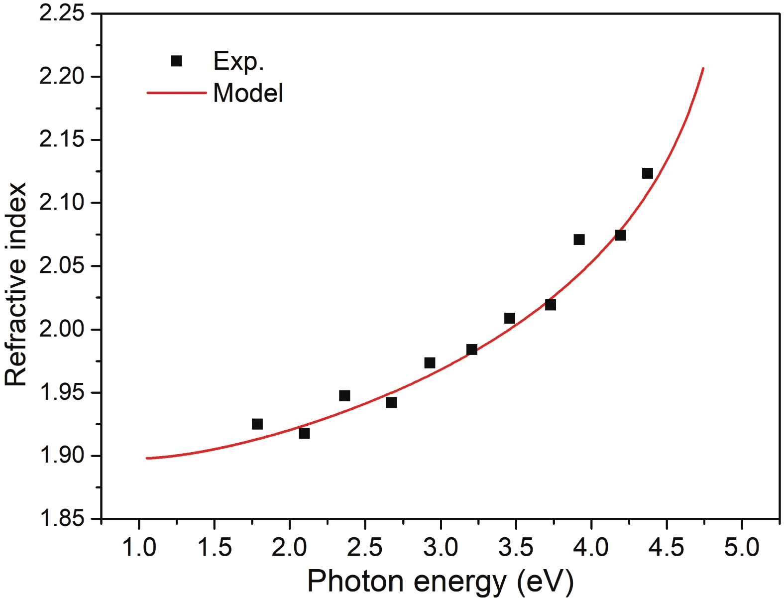
    Fig. 1 shows the calculated (solid line) and the experimental (solid squares) refractive indexes of β-Ga2O3 thin films as a function of photon energy. The experimental data were reported by Rebien et al.[17] for the β-Ga2O3 thin films deposited onto an epitaxial GaAs buffer layer (Si doping density 1.6 × 1016 cm−3) on (001)-oriented GaAs substrate wafers. X-ray diffraction revealed a nanocrystalline morphology of the thin films[17]. The theoretical line was calculated with Eq. (1). In the calculation, the parameters of 5.098 eV, 5.248 eV, and 4.893 eV were adopted. Here and shall be two material-dependent energy parameters, while should be an effective optical bandgap of material. As shown later, is dependent on doping concentration and lattice distortion degree. In addition, a background value of 1.319 was utilized for the dispersion calculation of sub-bandgap refractive index. This background refractive index may be understood as the static refractive index of material. Good agreement between experiment and model is achieved. Therefore, an explicit analytical expression is obtained as for the sub-bandgap refractive indexes of β-Ga2O3 thin film. It is obvious that the sub-bandgap refractive index of β-Ga2O3 thin film exhibits a peculiar dispersion on energy. From our understanding, defects and impurities play an important role in the determination of such dispersion of refractive index in the sub-bandgap energy region. It should be noted that monoclinic phase β-Ga2O3 single crystal can have anisotropic refractive indexes. For instance, Bhaumik et al. measured temperature-dependent refractive index along crystallographic [010] and a direction perpendicular to (100)-plane (c-axis) for monoclinic phase β-Ga2O3 single crystal grown by the optical floating zone technique[19]. They found that the refractive index was 1.9881 and 1.9568 along [010] and the direction perpendicular to the (100)-plane, respectively, at 407 nm and 30 °C. Since photons at 407 nm have energy of 3.047 eV, the calculated refractive index was ~1.975 in Fig. 1, which is between the two anisotropic values measured by Bhaumik et al.[19].

    (Color online) The experimental (solid squares) and calculated (solid line) refractive indexes of β-Ga2O3 thin film as a function of photon energy. The experimental data were from Ref. [17], while the solid line was fitted with Eq. (1).

    Figure 1.(Color online) The experimental (solid squares) and calculated (solid line) refractive indexes of β-Ga2O3 thin film as a function of photon energy. The experimental data were from Ref. [17], while the solid line was fitted with Eq. (1).

    Fig. 2 shows measured sub-bandgap transmission spectra (solid squares) of the Si-doped β-Ga2O3 thin films grown on c-plane sapphire substrates by Hu et al.[4]. The flow rates of SiH4 were 0.00, 0.04, 0.08, 0.12, 0.16, and 0.20 standard cubic centimeter per minute (sccm) for the six samples grown and measured by them. By utilizing the below dispersion relationship of refractive index in the sub-bandgap energy region proposed by Bao and Xu[18],

    (Color online) The measured transmission spectra (solid squares) and corresponding fitting curves (red solid lines) of the β-Ga2O3 thin films. The experimental spectra were measured by Hu et al.[4], while the fitting curves were obtained with Eq. (2) described in the text.

    Figure 2.(Color online) The measured transmission spectra (solid squares) and corresponding fitting curves (red solid lines) of the β-Ga2O3 thin films. The experimental spectra were measured by Hu et al.[4], while the fitting curves were obtained with Eq. (2) described in the text.

    $ n\left(E\right)=n_0+\frac{{E}_{1}-\sqrt{{E}_{2}\left({E}_{\mathrm{c}}-E\right)}}{E} , $  (1)

    where n0 is a background refractive index, i.e., static refractive index, the transmission spectrum of thin film due to the thin-film interference effect may be formulated as[18]

    $ {I}_{\mathrm{t}}={I}_{\mathrm{t}0}+{I}_{\mathrm{t}1}{\rm e}^{-\frac{8\pi dkE}{hc}}+2\sqrt{{I}_{\mathrm{t}0}{I}_{\mathrm{t}1}}{\rm e}^{-\frac{4\pi dkE}{hc}}\mathrm{cos}\left[\frac{4\pi d}{hc}\left({E}_{1}-\sqrt{{E}_{2}\left({E}_{\mathrm{c}}-E\right)}\right)\right] , $  (2)

    where is the intensity of the primary transmitted light, is the intensity of the first-order transmitted light after experiencing the double-round reflections inside the thin film, d is the film thickness, k is the extinction coefficient of the thin film, E is the photon energy, h is the Planck constant, is the light speed in vacuum, is the material dependent energy parameter, and is the effective optical bandgap of material. It should be noted that the whole phase variable in the cosine function of the interference term (i.e., the third term in the right-hand side of Eq. (2)) in Eq. (2) shows a particular dependence on photon energy (or wavelength), resulting in a variable-period oscillation pattern in the sub-bandgap energy (i.e., ).

    The solid lines in Fig. 2 represent the simulation curves with Eq. (2). Good agreement between theory and experiment is achieved, which leads to the determination of several key parameters such as the film thickness and effective optical bandgap. The determined thin film thickness was ~500 nm. It is regrettable that there were no experimental thickness data of the thin films reported in Ref. [4]. The obtained effective optical bandgap values are tabulated in Table 1. The experimental flow rates of SiH4 are listed in Table 1 too. From Table 1, the effective optical bandgap of intentionally undoped β-Ga2O3 thin film was 4.952 eV. Available bandgap values of β-Ga2O3 crystal are quite scattered, i.e., 4.7−5.04 eV, probably due to different theoretical approaches, doping concentrations, and crystal orientations[20-25]. The obtained value in the present study is well within the range of 4.7–5.04 eV. A clear tendency is the shrinking behavior of the effective optical bandgap with the flow rate of SiH4. For instance, when the flow rate was increased from 0 to 0.20 sccm, the effective optical bandgap decreases from 4.952 to 4.770 eV. Such tendency indicates that the effective optical bandgap of Si-doped β-Ga2O3 thin films shrinks with increasing the Si doping concentration. From our point of view, the shrinking of the effective bandgap with the rise of doping concentration is mainly due to the penetrating of wave functions of intrinsic electronic states at band maxima into bandgap under the action of electric fields induced by ionized dopants. As the dopant density increases, the average magnitude of electric fields increases and then results in the longer (deeper) penetration length. As a result, the effective bandgap shrinks.

    Table Infomation Is Not Enable

    It is well known that ionized dopants in solid can produce electric fields around them inside solid. Such ionized-dopant-induced electric fields may result in some significant effects, such as their substantial impact on the band-edge absorption of insulating solids[26-28]. Fig. 3 presents the measured (open circles) and theoretical (thin green line: Urbach model; thick red line: electric field effect) sub-bandgap absorption coefficients of β-Ga2O3 with impurity density of 2.52 × 1024 m−3. As the Urbach model is a widely used model in the calculation of sub-bandgap absorption spectrum, here we employed it to calculate the absorption spectrum of β-Ga2O3 for comparison. The experimental data were from Ref. [29]. By considering the effective optical bandgap of ~4.70 eV[30, 31], the sub-bandgap absorption coefficients of β-Ga2O3 were hence calculated for photon energies less than 4.7 eV. Note that the absorption coefficients were plotted in a semi-logarithmic scale in Fig. 3. For the electric field effect, the calculation formula of sub-bandgap absorption coefficient is as follows[28]

    (Color online) Measured (open circles) and calculated (solid lines) sub-bandgap absorption coefficients of β-Ga2O3 thin film with an impurity density of 2.52 × 1024 m–3. Note that the plot is drawn in a semi-logarithmic scale. The original experimental data was from Ref. [29].

    Figure 3.(Color online) Measured (open circles) and calculated (solid lines) sub-bandgap absorption coefficients of β-Ga2O3 thin film with an impurity density of 2.52 × 1024 m–3. Note that the plot is drawn in a semi-logarithmic scale. The original experimental data was from Ref. [29].

    $ \alpha \left(\omega ,F\right)=R\left(\omega \right)\frac{{\omega }_{\mathrm{F}}^{3/2}}{8\pi \left({\omega }_{\mathrm{g}}-\omega \right)}\mathrm{exp}\left[-\frac{4}{3}{\left(\frac{{\omega }_{\mathrm{g}}-\omega }{{\omega }_{\mathrm{F}}}\right)}^{3/2}\right] , $  (3)

    where , is the electron charge, comprises the matrix element having the dimensions of momentum, c is the light speed in vacuum, is the frequency-dependent refractive index, is the mass of free electron, , is the reduced mass with as the effective mass of the electrons (holes) in the conduction (valence) band. Here is defined as[28]

    $ {\omega }_{\mathrm{F}}={\left(\frac{{e}^{2}{F}^{2}}{12{\hslash }\mu }\right)}^{1/3} , $  (4)

    where is electric field induced by ionized dopants. Calculation formulas and descriptions of its magnitude (i.e., dependence on dopant concentration) and distribution (i.e., distance dependence) within a crystal can be referred to as in Ref. [28]. is the fundamental bandgap of the crystal. Note that the units of Eqs. (3) and (4) are the S.I. units. In the calculation of sub-bandgap absorption coefficient of β-Ga2O3 thin film, n = 2.14[18], [32], , m−3, and eV[30, 31] were adopted. For the effective mass of holes, its value has not been determined so far because of rather flat valence bands and anisotropy around Γ point. Herein, we tentatively assume that it is ten times of , much larger than the effective mass of electrons, i.e., as argued in Ref. [3335]. When the impurity atoms with density of m−3 are singly charged, the resulting average electric field was V/m. Clearly, the calculated absorption coefficients are in good agreement with the experimental data for photon energies <4.70 eV. However, a larger deviation between the theoretical Urbach line [36] and the experimental data exists. These results advocate that the electric fields induced by ionized Si impurities could be the major factor of sub-bandgap absorption in doped β-Ga2O3 thin films. As a final remarking note, we would like to point out that the sub-bandgap electronic states and optical properties in WBG semiconductors may be more complicated than the present understanding, for instance, the recent observation of the long persistent phosphorescence in the sub-bandgap region in ZnO under the sub-bandgap excitation[37, 38]. Further investigation about this issue needs to be done.

    3. Conclusions

    In conclusion, the dispersion of the refractive index of β-Ga2O3 thin film in the sub-bandgap energy region was elucidated. Based on the peculiar dispersion of sub-bandgap refractive index, the variable-period oscillation patterns in the measured sub-bandgap transmission spectra of Si-doped β-Ga2O3 thin films with different doping concentrations were quantitatively interpreted. It is found that the effective optical bandgap of the films decreases with increasing the Si doping concentration. Under the frame of Franz–Keldysh mechanism due to the electric fields, the sub-bandgap absorption coefficients of β-Ga2O3 were calculated. It is shown that the electric fields induced by ionized Si impurities should be responsible for the sub-bandgap absorption in β-Ga2O3 thin films. These new findings not only deepen the existing understanding of the sub-bandgap refractive indexes and optical properties of β-Ga2O3, but also may promote the further device applications of this unique WBG oxide semiconductor.

    Acknowledgements

    This study was financially supported by the National Natural Science Foundation of China (No. 12074324) and the Shenzhen Municipal Science and Technology Innovation Council (No. JCJY20180508163404043).

    References

    [1] S J Pearton, J Yang, IV P H Cary et al. A review of Ga2O3 materials, processing, and device. Appl Phys Rev, 5, 011301(2018).

    [2] H F Mohamed, C Xia, Q Sai et al. Growth and fundamentals of bulk β-Ga2O3 single crystals. J Semicond, 40, 011801(2019).

    [3] F Zhang, M Arita, X Wang et al. Toward controlling the carrier density of Si doped Ga2O3 films by pulsed laser deposition. Appl Phys Lett, 109, 102105(2016).

    [4] D Hu, Y Wang, S Zhuang et al. Surface morphology evolution and optoelectronic properties of heteroepitaxial Si-doped β-Ga2O3 thin films grown by metal-organic chemical vapor deposition. Ceram Internation, 44, 3122(2018).

    [5] S J Pearton, F Ren, M Tadjer et al. Perspective: Ga2O3 for ultra-high power rectifiers and MOSFETS. J Appl Phys, 124, 220901(2018).

    [6] J Yang, S Ahn, F Ren et al. High breakdown voltage (−201) β-Ga2O3 Schottky rectifiers. IEEE Electron Device Lett, 38, 906(2017).

    [7] B Wang, M Xiao, X Yan et al. High-voltage vertical Ga2O3 power rectifiers operational at high temperatures up to 600 K. Appl Phys Lett, 115, 263503(2019).

    [8] K D Chabak, J P McCandless, N A Moser et al. Recessed-gate enhancement-mode β-Ga2O3 MOSFETs. IEEE Electron Device Lett, 39, 67(2018).

    [9] A J Green, K D Chabak, M Baldini et al. β-Ga2O3 MOSFETs for radio frequency operation. IEEE Electron Device Lett, 38, 790(2017).

    [10] N Moser, J McCandless, A Crespo et al. Ge-doped β-Ga2O3 MOSFETs. IEEE Electron Device Lett, 38, 775(2017).

    [11] S Oh, C K Kim, J Kim. High responsivity β-Ga2O3 metal–semiconductor–metal solar-blind photodetectors with ultraviolet transparent graphene electrodes. ACS Photon, 5, 1123(2018).

    [12] Y C Chen, Y J Lu, Q Liu et al. Ga2O3 photodetector arrays for solar-blind imaging. J Mater Chem C, 7, 2557(2019).

    [13] J Xu, W Zheng, F Huang. Gallium oxide solar-blind ultraviolet photodetectors: a review. J Mater Chem C, 7, 8753(2019).

    [14] Z Liu, X Wang, Y Liu et al. A high-performance ultraviolet solar-blind photodetector based on a β-Ga2O3 Schottky photodiode. J Mater Chem C, 7, 13920(2019).

    [15] L Zhang, X Xiu, Y Li et al. Solar-blind ultraviolet photodetector based on vertically aligned single-crystalline β-Ga2O3 nanowire arrays. Nanophotonics, 9, 0295(2020).

    [16] C Xie, X Lu, Y Liang et al. Patterned growth of β-Ga2O3 thin films for solar-blind deep-ultraviolet photodetectors array and optical imaging application. J Mater Sci Technol, 72, 189(2021).

    [17] M Rebien, W Henrion, M Hong et al. Optical properties of gallium oxide thin films. Appl Phys Lett, 81, 250(2002).

    [18] Y Bao, S Xu. Variable-period oscillations in optical spectra in sub-bandgap long wavelength region: Signatures of new dispersion of refractive index. J Phys D, 54, 155102(2021).

    [19] I Bhaumik, R Bhatt, S Ganesamoorthy et al. Temperature-dependent index of refraction of monoclinic Ga2O3 single crystal. Appl Opt, 50, 6006(2011).

    [20] N Ueda, H Hosono, R Waseda et al. Anisotropy of electrical and optical properties in β-Ga2O3 single crystals. Appl Phys Lett, 71, 933(1997).

    [21] M Hilfiker, U Kilic, A Mock et al. Dielectric function tensor (1.5 eV to 9.0 eV), anisotropy, and band to band transitions of monoclinic β-(AlxGa1–x)2O3 (x ≤ 0.21) films. Appl Phys Lett, 114, 231901(2019).

    [22] J Furthmüller, F Bechstedt. Quasiparticle bands and spectra of Ga2O3 polymorphs. Phys Rev B, 93, 115204(2016).

    [23] J Yan, C Qu. Electronic structure and optical properties of F-doped-Ga2O3 from first principles calculations. J Semicond, 37, 042002(2016).

    [24] A Mock, R Korlacki, C Briley et al. Band-to-band transitions, selection rules, effective mass, and excitonic contributions in monoclinic β-Ga2O3. Phys Rev B, 96, 245205(2017).

    [25] Z Galazka. β-Ga2O3 for wide-bandgap electronics and optoelectronics. Semicond Sci Technol, 33, 113001(2018).

    [26] D Redfield. Effect of defect fields on the optical absorption edge. Phys Rev, 130, 916(1963).

    [27] K Tharmalingam. Optical absorption in the presence of a uniform field. Phys Rev, 130, 2204(1963).

    [28] Y Bao, S Xu. Dopant-induced electric fields and their influence on the band-edge absorption of GaN. ACS Omega, 4, 15401(2019).

    [29] S Rafique, L Han, S Mou et al. Temperature and doping concentration dependence of the energy band gap in β-Ga2O3 thin films grown on sapphire. Opt Mater Express, 7, 3561(2017).

    [30] R Subrina, L Han, H Zhao. Synthesis of wide bandgap Ga2O3 (Eg ~ 4.6–4.7 eV) thin films on sapphire by low pressure chemical vapor deposition. Phys Status Solidi A, 213, 1002(2016).

    [31] J Zhang, J Shi, D C Qi et al. Recent progress on the electronic structure, defect, and doping properties of Ga2O3. APL Mater, 8, 020906(2020).

    [32] H Peelaers, C G Van de Walle. Sub-band-gap absorption in Ga2O3. Appl Phys Lett, 111, 182104(2017).

    [33] F Bechstedt, J Furthmüller. Influence of screening dynamics on excitons in Ga2O3 polymorphs. Appl Phys Lett, 114, 122101(2019).

    [34] R Guo, J Su, H Yuan et al. Surface functionalization modulates the structural and optoelectronic properties of two-dimensional Ga2O3. Mater Today Phys, 12, 100192(2020).

    [35] S L Shi, S J Xu. Determination of effective mass of heavy hole from phonon-assisted excitonic luminescence spectra in ZnO. J Appl Phys, 109, 053510(2011).

    [36] X Wang, D Yu, S Xu. Determination of absorption coefficients and Urbach tail depth of ZnO below the bandgap with two-photon photoluminescence. Opt Express, 28, 13817(2020).

    [37] H G Ye, Z C Su, F Tang et al. Role of free electrons in phosphorescence in n-type wide bandgap semiconductors. Phys Chem Chem Phys, 19, 30332(2017).

    [38] H Ye, Z Su, F Tang et al. Probing defects in ZnO by persistent phosphorescence. Opto-Electron Adv, 1, 180011(2018).

    Yitian Bao, Xiaorui Wang, Shijie Xu. Sub-bandgap refractive indexes and optical properties of Si-doped β-Ga2O3 semiconductor thin films[J]. Journal of Semiconductors, 2022, 43(6): 062802
    Download Citation