• Chinese Optics Letters
  • Vol. 19, Issue 3, 031401 (2021)
Zixin Yang1、4, Lili Han1, Qi Yang1、3、*, Xianghe Ren1、**, Syed Zaheer Ud Din1, Xiaoyan Zhang2、***, Jiancai Leng4, Jiabao Zhang1、4, Baitao Zhang3, Kejian Yang3, Jingliang He3, Chunlong Li5, and Jun Wang6
Author Affiliations
  • 1International School for Optoelectronic Engineering, Qilu University of Technology (Shandong Academy of Sciences), Jinan 250300, China
  • 2Department of Chemistry, Shanghai University, Shanghai 200444, China
  • 3State Key Laboratory of Crystal Materials, Shandong University, Jinan 250100, China
  • 4School of Electronic and Information Engineering (Department of Physics), Qilu University of Technology (Shandong Academy of Sciences), Jinan 250300, China
  • 5State Key Laboratory of Biobased Material and Green Papermaking, Qilu University of Technology (Shandong Academy of Sciences), Jinan 250300, China
  • 6Key Laboratory of Materials for High-Power Laser, Shanghai Institute of Optics and Fine Mechanics, Chinese Academy of Sciences, Shanghai 201800, China
  • show less
    DOI: 10.3788/COL202119.031401 Cite this Article Set citation alerts
    Zixin Yang, Lili Han, Qi Yang, Xianghe Ren, Syed Zaheer Ud Din, Xiaoyan Zhang, Jiancai Leng, Jiabao Zhang, Baitao Zhang, Kejian Yang, Jingliang He, Chunlong Li, Jun Wang. Two-dimensional tellurium saturable absorber for ultrafast solid-state laser[J]. Chinese Optics Letters, 2021, 19(3): 031401 Copy Citation Text show less
    Fabrication process of Te SA.
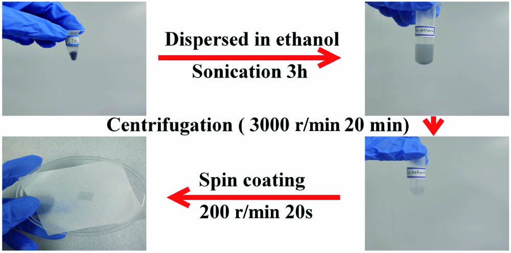
    Fig. 1. Fabrication process of Te SA.
    (a) AFM image of Te SA at the scales of 5 µm. (b) The typical height profiles of Te SAs in a larger area. (c) AFM image of Te SAs at the scales of 1 µm. (d) The typical height profiles of Te SAs in a smaller area.
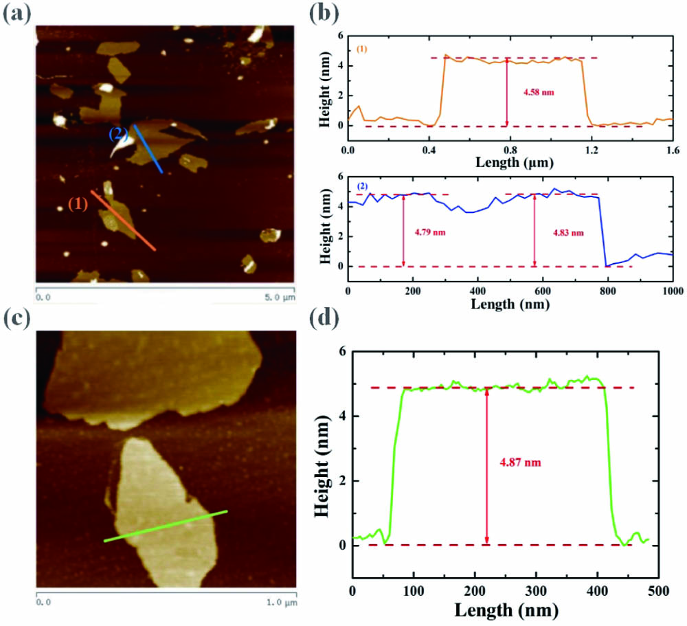
    Fig. 2. (a) AFM image of Te SA at the scales of 5 µm. (b) The typical height profiles of Te SAs in a larger area. (c) AFM image of Te SAs at the scales of 1 µm. (d) The typical height profiles of Te SAs in a smaller area.
    (a) XRD pattern of Te. (b) Raman spectrum of Te SA. (c) TEM image of Te samples. (d) High-resolution (HR) TEM image of Te samples.
    Fig. 3. (a) XRD pattern of Te. (b) Raman spectrum of Te SA. (c) TEM image of Te samples. (d) High-resolution (HR) TEM image of Te samples.
    (a) Normalized transmittance versus z axis at the excitation pulse energy of 100 nJ. (b) The nonlinear transmission versus energy intensity of Te SAs.
    Fig. 4. (a) Normalized transmittance versus z axis at the excitation pulse energy of 100 nJ. (b) The nonlinear transmission versus energy intensity of Te SAs.
    Schematic of the mode-locked laser setup based on Te SA.
    Fig. 5. Schematic of the mode-locked laser setup based on Te SA.
    (a) Average output power versus absorbed pump power of the mode-locked solid-state laser. (b) The typical QML pulse trains recorded on different time scales. (c) The typical CWML pulse trains recorded on different time scales. (d) Autocorrelation trace for 5.8 ps duration. Inset, the corresponding spectrum centered at 1064.3 nm.
    Fig. 6. (a) Average output power versus absorbed pump power of the mode-locked solid-state laser. (b) The typical QML pulse trains recorded on different time scales. (c) The typical CWML pulse trains recorded on different time scales. (d) Autocorrelation trace for 5.8 ps duration. Inset, the corresponding spectrum centered at 1064.3 nm.
    SAGain MediumPulse Width [ps]Pulse Energy [nJ]Peak Power [kW]Ref.
    SWCNTsNd:YVO47.637.54.9[4]
    GrapheneNd:GdVO4168.40.53[6]
    PtSe2Nd:LuVO415.82.940.19[11]
    BPNd:YVO46.13.290.54[14]
    TeNd:YVO45.88.481.46This work
    Table 1. Comparison of 1 µm CWML Laser Characteristics Based on Different SAs
    Zixin Yang, Lili Han, Qi Yang, Xianghe Ren, Syed Zaheer Ud Din, Xiaoyan Zhang, Jiancai Leng, Jiabao Zhang, Baitao Zhang, Kejian Yang, Jingliang He, Chunlong Li, Jun Wang. Two-dimensional tellurium saturable absorber for ultrafast solid-state laser[J]. Chinese Optics Letters, 2021, 19(3): 031401
    Download Citation