1International School for Optoelectronic Engineering, Qilu University of Technology (Shandong Academy of Sciences), Jinan 250300, China
2Department of Chemistry, Shanghai University, Shanghai 200444, China
3State Key Laboratory of Crystal Materials, Shandong University, Jinan 250100, China
4School of Electronic and Information Engineering (Department of Physics), Qilu University of Technology (Shandong Academy of Sciences), Jinan 250300, China
5State Key Laboratory of Biobased Material and Green Papermaking, Qilu University of Technology (Shandong Academy of Sciences), Jinan 250300, China
6Key Laboratory of Materials for High-Power Laser, Shanghai Institute of Optics and Fine Mechanics, Chinese Academy of Sciences, Shanghai 201800, China
Two-dimensional (2D) Te nanosheets were successfully fabricated through the liquid-phase exfoliation (LPE) method. The nonlinear optical properties of 2D Te nanosheets were studied by the open-aperture Z-scan technique. Furthermore, the continuous wave mode-locked Nd:YVO4 laser was successfully realized by using 2D Te as a saturable absorber (SA) for the first time, to the best of our knowledge. Ultrashort pulses as short as 5.8 ps were obtained at 1064.3 nm with an output power of 851 mW. This primary investigation indicates that the 2D Te SA is a promising photonic device in the fields of ultrafast solid-state lasers.
Two-dimensional (2D) materials have attracted tremendous attention over the past decade due to their outstanding electronic and optical properties, which have been widely used in diverse fields such as energy storage, electroluminescent, transistors, photonics, and biology[1–7]. Around 2009, graphene was initially found to have excellent nonlinear optical properties[8]. Stimulated by the success of graphene, other 2D materials such as transition metal dichalcogenides (TMDs)[9–11], topological insulators[12], black phosphorus (BP)[13–15], gold nanomaterials[16–18], MXenes[19], graphyne[20], and epsilon-near-zero (ENZ) materials[21] have been intensively researched due to their excellent nonlinear optical properties. Among the various 2D materials, graphene has a broad operation wavelength band, but its weak absorption limits its applications in optoelectronic devices. TMDs have a tunable bandgap and high carrier mobility, which have a chemical formula of (where , Se, etc., and , W, Re, etc.). However, the intrinsic energy bandgap of TMDs is in , which limits their optoelectronic applications over mid-infrared bands. BP exhibits an outstanding optical modulation effect, but it is easily oxidized, which may cause dramatic structural transformations. Thus, it is still necessary to make efforts to explore novel 2D materials suitable for photonic devices. As the group VI elemental material, tellurium (Te) has attracted extensive attention because of its distinctive properties, e.g., thermoelectricity, photoconductivity, and piezoelectricity[22–24]. For example, Cao et al.[25] reported the solar-blind deep ultraviolet photodetectors based on Te nanosheets in 2020, which indicate the great potential of Te nanosheets for high-performance photodetectors. Elemental Te ordinarily forms a trigonal crystal structure consisting of atomic chains that spiral along with one of the axes of the crystal lattice. Due to the weak van der Waals interactions, these helical chains are collected together to construct hexagonal lattices, leading to the generation of one-dimensional (1D) Te nanostructures, such as nanowires[26], nanotubes[27], and nanobelts[28]. Compared with 1D nanostructures, 2D Te has the large specific surface area and thickness-modulated band gap, which further endows the surface with broader application prospects.
In recent years, the -Te, -Te, and -Te phases have been reported, demonstrating that the carrier mobility of three 2D Te phases is superior to [29–32]. Furthermore, Te with a bandgap of about 0.35 eV at room temperature is a -type semiconductor with a configuration. Its narrow energy bandgap is comparable to BP, opening the possibilities for optoelectronic applications at broadband wavelengths, especially at the infrared wavelength. Very recently, Te has been proved to be a potential saturable material in generating -switched and mode-locked pulsed lasers. For example, by using the Te saturable absorber (SA), Wang et al.[33] successfully realized the erbium-doped mode-locked fiber laser at 1.55 µm in 2019, with the shortest pulse width of 1.81 ps and the maximum output power of 1.95 mW. In 2020, Hassan et al.[34] applied the Te nanorod as an SA to realize the erbium-doped mode-locked fiber laser at 1.57 µm. Pulses with a minimum pulse width of 3.56 ps and the maximum output power of 6.2 mW were achieved in their work. Compared with fiber lasers, solid-state lasers can realize higher peak power. Unfortunately, the potential of Te as an SA in solid-state lasers of the near-infrared region has not yet been explored.
In this work, we systematically studied the nonlinear optical properties of 2D Te nanosheets, and the results exhibited the promising application of Te in ultrafast photonics. Furthermore, by using 2D Te as the SA, the continuous wave mode-locked (CWML) solid-state laser at 1.06 µm was successfully realized for the first time, to the best of our knowledge. This research work broadens the applied spectral ranges of Te and shows that 2D Te SAs could be a promising optical modulator for ultrafast solid-state lasers.
Sign up for Chinese Optics Letters TOC. Get the latest issue of Chinese Optics Letters delivered right to you!Sign up now
2. Preparation and Characterization of 2D Te Nanosheets
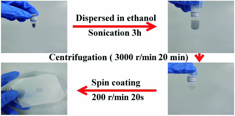
The 2D Te nanosheets were fabricated by the liquid-phase exfoliation (LPE) method. This method has been demonstrated to be a simple and effective way to fabricate 2D materials. As shown in Fig. 1, the Te powder with purity of 99.99%, which was synthesized by a chemical method, was dispersed in an alcohol suspension and ultrasonicated for 3 h to fabricate thin nanosheets. The ultrasonic process was operated at a suitable interval to avoid the change of the material properties under high temperature. After that, the as-prepared suspension was centrifuged at 3000 r/min for 20 min to remove aggregated powders. Finally, the extracted Te supernatant was transferred onto a sapphire substrate by spin coating at 200 r/min for 20 s and dried under an infrared oven lamp. In order to investigate the thickness and distribution of the 2D Te nanosheets located on the sapphire substrate, an atomic force microscope (AFM) was used to study the morphology of the as-prepared Te SA. The AFM images of the sample at the scales of 5 µm and 1 µm are given in Figs. 2(a) and 2(c), showing the sheet structure of the as-prepared Te SA. The average thickness of the Te nanosheets was determined to be about 5 nm [see Figs. 2(b) and 2(d)], and the corresponding number of layers of the Te nanosheets is about 12[35].
Figure 2.(a) AFM image of Te SA at the scales of 5 µm. (b) The typical height profiles of Te SAs in a larger area. (c) AFM image of Te SAs at the scales of 1 µm. (d) The typical height profiles of Te SAs in a smaller area.
The crystal phases of the Te sample were systematically characterized by employing X-ray diffraction (XRD) and Raman techniques. The XRD pattern of Te is presented in Fig. 3(a), and the strongest diffraction peak is located at 27.57°, which corresponds to the (101) planes. The Raman spectrum in the wavenumber range (with a 532 nm laser as the excited source) of the Te sample is acquired and plotted in Fig. 3(b). Two conspicuous Raman peaks located at and are assigned to the first-order vibration modes of bending and stretching in the Te crystal. The peak located at is the second-order Raman vibration. Except for these modes, the bands, which are located at , , and , can be contributed from the small amount of oxidation of Te(0)[33]. The experimental results of XRD and Raman spectra indicated that the prepared Te nanosheets had good crystallinity. Figure 3(c) shows the typical transmission electron microscopy (TEM) image of the Te sample, which depicts it to be a thin sheet with a size of about 450 nm. The lattice structure of Te nanosheets was further determined by high-resolution (HR) TEM (HRTEM). The lattice fringe spacings of 0.38 nm and 0.23 nm were observed corresponding to (101) and (102) lattice planes, as shown in Fig. 3(d).
Figure 3.(a) XRD pattern of Te. (b) Raman spectrum of Te SA. (c) TEM image of Te samples. (d) High-resolution (HR) TEM image of Te samples.
The nonlinear optical properties of the 2D Te nanosheets were measured by the open-aperture Z-scan technique. The laser source was a femtosecond laser at 1030 nm with a pulse width of 350 fs and a repetition rate of 1 kHz. Figure 4(a) shows the measured open-aperture Z-scan curves of the 2D Te SA under the excitation pulse energy of 100 nJ. The normalized transmittance gradually increases when the Te sample moves towards , indicating strong saturable absorption. To further study the nonlinear saturable absorption properties of the 2D Te SA, we fitted the data to a simple saturable absorption model:where is the transmittance rate, is the input intensity, and , , and are the modulation depth, saturation intensity, and nonsaturable loss, respectively. Figure 4(b) presents the nonlinear transmittance curve versus the energy intensity. The modulation depth and saturation intensity of the Te SA were calculated to be 1.9% and , respectively.
Figure 4.(a) Normalized transmittance versus z axis at the excitation pulse energy of 100 nJ. (b) The nonlinear transmission versus energy intensity of Te SAs.
To further investigate the ability of 2D Te to generate ultrafast pulses, its application in a mode-locked solid-state laser at 1.06 µm is studied. The experimental setup of the Te-based mode-locked laser is shown in Fig. 5. A crystal was chosen as the gain medium. By considering the parameters of the crystal and SA, a 1.495 m long W-type optimum resonator was designed in our experiment, corresponding to the round-trip time of 9.97 ns. and were the planar mirrors, while and were the concave mirrors with curvature radii of 200 and 800 mm, respectively. They all had an antireflection (AR) coating for the pump light (808 nm) and an HR coating for oscillating light (1064 nm). The output coupler with the curvature radii of 100 mm had a transmission of 1% at 1064 nm. For the CWML laser experiment, the prepared Te SA was inserted into the cavity near . Based on the ABCD matrix, the laser mode radii on Nd: and Te SA were determined to be 104 µm and 31 µm.
Figure 5.Schematic of the mode-locked laser setup based on Te SA.
The average output power versus absorbed pump power is shown in Fig. 6(a). As the absorbed pump power increased to 3.84 W, the laser mode changed from CW to Q-switched mode-locking (QML) operation. When the absorbed pump power increased to 6.44 W, the laser ran into a stable CWML regime, corresponding to the output power of 442 mW. The maximum average output power of CWML was 851 mW under the absorbed pump power of 9.75 W with a slope efficiency of 9.3%. Figures 6(b) and 6(c) show the typical pulse trains of QML and CWML at the time scales of 200 ns and 10 µs, respectively. The measured repetition rate of the mode-locked operation was 100.3 MHz, which was in good agreement with the round-trip time. The jitter of the average output power (output powers, rms) at the maximum absorbed pump power was measured to be less than 1% at 1 h, indicating good stability of the CWML laser.
Figure 6.(a) Average output power versus absorbed pump power of the mode-locked solid-state laser. (b) The typical QML pulse trains recorded on different time scales. (c) The typical CWML pulse trains recorded on different time scales. (d) Autocorrelation trace for 5.8 ps duration. Inset, the corresponding spectrum centered at 1064.3 nm.
Figure 6(d) displays the autocorrelation trace of the laser pulse, where the pulse duration was measured to be 5.8 ps by pulse shape fitting. The emitted optical spectrum of the CWML laser under the maximum output power is depicted in the inset of Fig. 6(d). The spectral FWHM of the mode-locked laser was about 0.30 nm with a central wavelength at 1064.3 nm. According to the above data, the maximum obtained pulse energy and peak power were calculated to be 8.48 nJ and 1.46 kW, respectively. Based on the mode-locking theory, the relationship between laser dynamics and mode lockers to realize stable passively mode-locked operation can be expressed as[36]where is the energy of a mode-locked pulse in the cavity, is the intracavity pulsed laser power, is the round-trip time, is the critical intracavity pulse energy, and and are the saturation energies of the laser gain material and SA, respectively. When , the stable CWML operation can be obtained. To make the relationship between laser dynamics and mode-locked laser more obvious, can be computed by the following equation[36]:where is the saturation fluence of the laser medium, is the emission cross section of the laser crystal, , , and are the laser wavelength, the Planck constant, and the light velocity, respectively, and is the cavity constant, with for a ring cavity and for a linear cavity. and are the effective laser mode areas on the crystal and SA; and are the laser spot radius of the crystal and SA; respectively. Based on the above data, was calculated to be , and was calculated to be . It matches the relation of , indicating that stable CWML operation was obtained.
Table 1 exhibits typical pulse parameters of the CWML lasers at 1.06 µm by using various SAs, such as single-walled carbon nanotubes (SWCNTs)[4], graphene[6], [11], and BP[14]. The pulse energy and peak power in this work were inferior to SWCNTs, but better than other nanomaterials. In addition, the pulse width, which was realized based on the 2D Te SA, is the shortest among the materials mentioned above. It can be concluded that the 2D Te SA is an excellent optical modulator for solid-state ultrafast laser generation. The maximum peak power intensity on the SA was calculated to be about , and we did not find any optical damage on the Te SA in the laser experiment, which indicates that the damage threshold of Te for an ultrafast laser should be larger than . The time-bandwidth product was about 0.455, which was higher than the Fourier transform limit of 0.315. It indicates that the mode-locked pulse was chirped, and we can further compress the pulse duration by optimizing the laser cavity configuration and compensating the dispersion in future work.
SA
Gain Medium
Pulse Width [ps]
Pulse Energy [nJ]
Peak Power [kW]
Ref.
SWCNTs
Nd:YVO4
7.6
37.5
4.9
[4]
Graphene
Nd:GdVO4
16
8.4
0.53
[6]
PtSe2
Nd:LuVO4
15.8
2.94
0.19
[11]
BP
Nd:YVO4
6.1
3.29
0.54
[14]
Te
Nd:YVO4
5.8
8.48
1.46
This work
Table 1. Comparison of 1 µm CWML Laser Characteristics Based on Different SAs
In conclusion, the 2D Te nanosheets were successfully synthesized by using the LPE method. The nonlinear optical properties of 2D Te nanosheets were investigated by applying the open-aperture Z-scan technique. The results proved that 2D Te nanosheets have excellent nonlinear optical properties. Furthermore, we successfully realized the CWML laser by using the 2D Te SA for the first time, to the best of our knowledge. Pulses as short as 5.8 ps with a repetition rate of 100.3 MHz and maximum output power of 851 mW were achieved at the central wavelength of 1064.3 nm. Our research work indicates that the 2D Te SA could be an excellent optical modulator and may be beneficial for the design of 2D optoelectronic devices.