
Xiangdong Li, Karen Geens, Nooshin Amirifar, Ming Zhao, Shuzhen You, Niels Posthuma, Hu Liang, Guido Groeseneken, Stefaan Decoutere. Integration of GaN analog building blocks on p-GaN wafers for GaN ICs[J]. Journal of Semiconductors, 2021, 42(2): 024103
- Journal of Semiconductors
- Vol. 42, Issue 2, 024103 (2021)
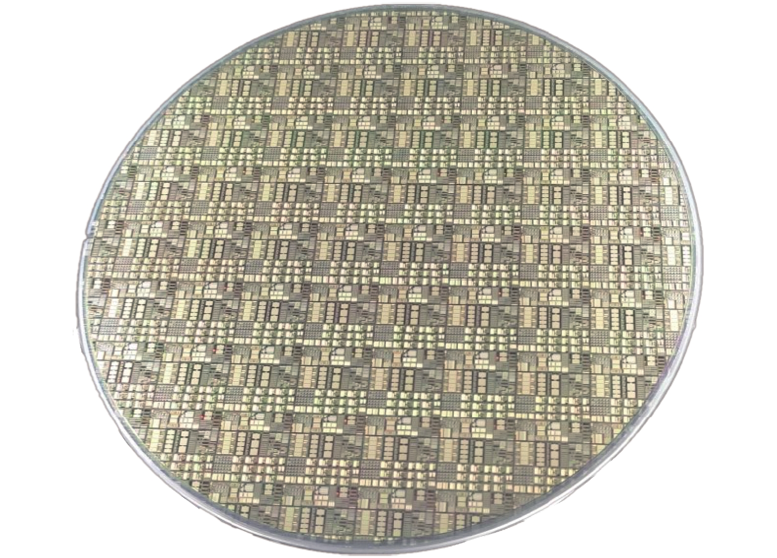
Fig. 1. (Color online) Fabricated 200 mm GaN-on-SOI wafer with CMOS-compatible processing.
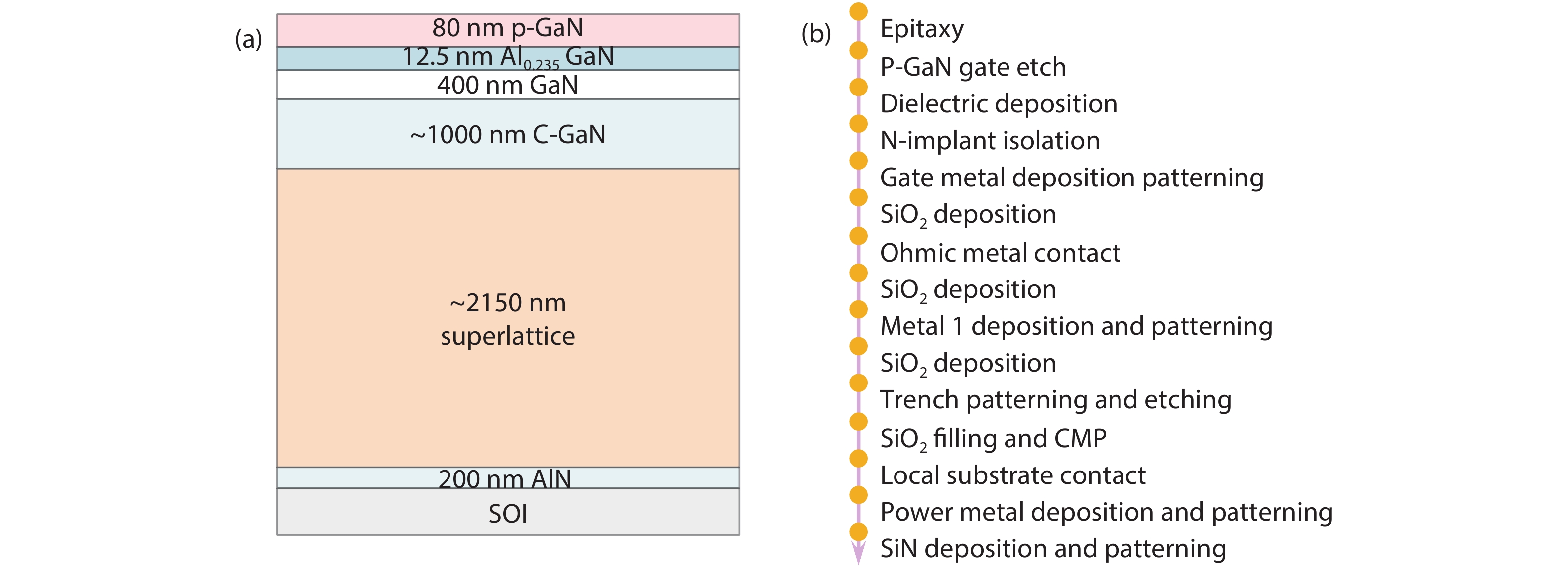
Fig. 2. (Color online) (a) Schematic cross-section of the epitaxial layer stack and (b) processing flow.
Fig. 3. (Color online) (a) Microscope images, (b) transfer characteristics, and (c) OFF-state leakage characteristics of the logic HEMTs with L GD of 1.5 μ m and W G scaling from 6 μ m to 2 μ m.
Fig. 4. (Color online) (a) Microscope image, (b) schematic, and (c) measured voltage transfer characteristic (VTC) of the integrated RTL inverter.
Fig. 5. (Color online) (a) Comparator designed by RTL and (b) the microscope image of the processed comparator.
Fig. 6. (Color online) (a) Voltage transfer characteristics of the comparator with (a) various V DD and (b) various reference voltage V REF.
Fig. 7. (Color online) (a) Undervoltage lockout GaN circuit, (b) layout, and (c) voltage transfer characteristics show the IC shuts down when V DD < 5 V and restarts when V DD > 5.7 V.

Set citation alerts for the article
Please enter your email address
© Copyright 2018-2021 | Chinese Laser Press. All Rights Reserved 沪ICP备15018463号-20