
Xiangdong Li, Karen Geens, Nooshin Amirifar, Ming Zhao, Shuzhen You, Niels Posthuma, Hu Liang, Guido Groeseneken, Stefaan Decoutere. Integration of GaN analog building blocks on p-GaN wafers for GaN ICs[J]. Journal of Semiconductors, 2021, 42(2): 024103
- Journal of Semiconductors
- Vol. 42, Issue 2, 024103 (2021)
Abstract
1. Introduction
GaN power ICs bear significant advantages over the discrete solution, namely reduced chip size, suppressed parasitic inductance, and simplified circuit designing[
Moreover, analog building blocks such as protection and diagnostic circuits are also obligatory. A comparator, the core block of analog ICs, is of paramount importance and has been demonstrated on D-mode epitaxy wafers[
2. Epitaxy and fabrication
This work commenced with device stack epitaxy using a MOCVD reactor on 200 mm SOI substrates, as shown in Fig. 1. The schematic cross-section is illustrated in Fig. 2(a). The epi stack consists of a 200 nm AlN nucleation layer, a 2.15 μm (Al)GaN buffer layer, a 400 nm GaN channel layer, a 12.5 nm Al0.235GaN barrier layer, and an 80 nm Mg-doped p-GaN layer. An in-situ annealing of the p-GaN layer was conducted in N2 ambient after the epitaxy to activate the Mg dopants. Delicate strain engineering was carried out in order to control the stress during the epitaxy and to avoid excessive wafer warp. The optimized epi stack showed a high structural quality with wafer warpage well below 50 μm and a smooth surface.
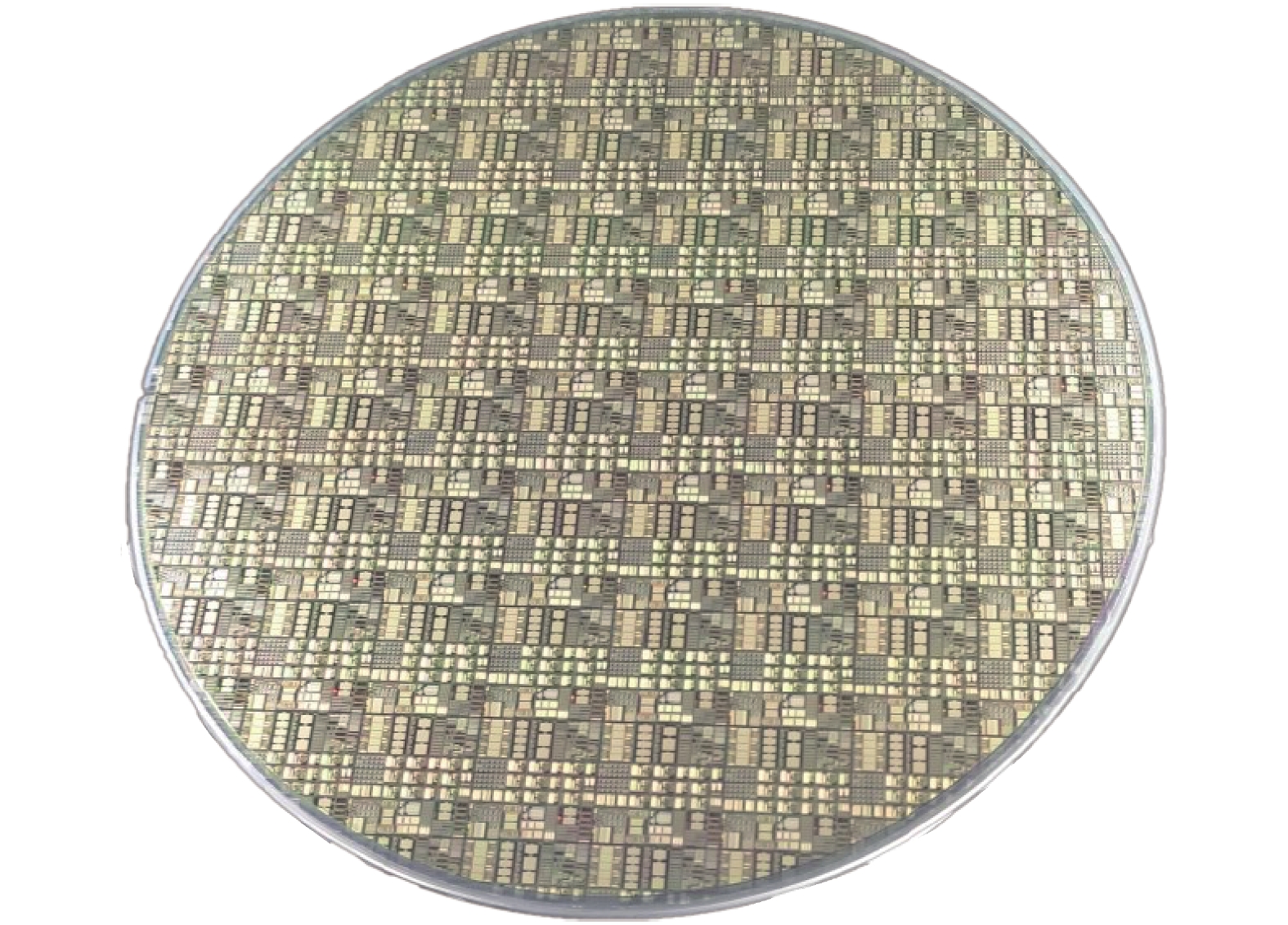
![]()
Figure 1.(Color online) Fabricated 200 mm GaN-on-SOI wafer with CMOS-compatible processing.
![]()
Figure 2.(Color online) (a) Schematic cross-section of the epitaxial layer stack and (b) processing flow.
The devices were processed using imec’s 200 mm CMOS compatible process modules and the processing flow is sequentially detailed in Fig. 2(b)[
Currently, p-GaN gate HEMT technology cannot fabricate complementary devices. Therefore, our integration falls back to the RTL that uses a 2DEG resistor to replace the pFET. The 2DEG resistor was fabricated together with the HEMTs. The p-GaN layer was first removed, followed by dielectric deposition. Then the two terminals of a 2DEG resistor were contacted by ohmic contacts. The fabricated HEMTs feature a small WG scaling down from 6 to 2 μm and a LGD of 1.5 μm as shown in Fig. 3. The 2-μm-wide meander 2DEG resistor works as a load resistor in the ICs. The RTL-based comparator and UVLO circuits were designed using the PDK of Ref. [15].
![]()
Figure 3.(Color online) (a) Microscope images, (b) transfer characteristics, and (c) OFF-state leakage characteristics of the logic HEMTs with
3. Results and discussion
The processed logic HEMTs show a VTH of ~ 3.6 V and IDS scaling with WG till 2 μm (Fig. 3(b)). The current bump on the ID–VGS curve at 1 V in Fig. 3(b) is stemming from the trapping effect of the p-GaN layer. In detail, when the gate is positively biased, the traps get charged so that the VGSwill drop on the p-GaN layer instead of the channel, which induce the current bump. This phenomenon has been elaborated in our previous work[
![]()
Figure 4.(Color online) (a) Microscope image, (b) schematic, and (c) measured voltage transfer characteristic (VTC) of the integrated RTL inverter.
Fig. 5 shows the comparator circuit and microscope image based on RTL inverters. Due to the lack of pFET, the gain, namely dVO/dVIN, of the RTL inverter is lower than that of the CMOS inverter, which is demonstrated by the smooth flipping curve in Fig. 4(c). To overcome this weakness, three-stage comparators are designed. In Fig. 6(a), a supply voltage VDD ranging from 3 to 7 V was sequentially applied to the comparator and the input signal VIN swept from 0 to 7 V. As can be seen, the comparator cannot work until the VDD reaches 5 V, suggesting the supply voltage VDD should be kept within 5 to 6 V, considering both the function and power dissipation. The basic function of this comparator is realized as shown in Fig. 6(b) where the VOflips at the corresponding VREF.
![]()
Figure 5.(Color online) (a) Comparator designed by RTL and (b) the microscope image of the processed comparator.
![]()
Figure 6.(Color online) (a) Voltage transfer characteristics of the comparator with (a) various
A UVLO circuit based on this comparator was further designed (Fig. 7(a)) and processed (Fig. 7(b)). UVLO is an electronic circuit used to turn off the power of an electronic device in the event of the voltage, battery charge for instance, dropping below the minimum operational value. Without this, logic functions may generate wrong control signals. Fig. 7(c) shows that when the VDD gradually ramps down to 5 V, the protection circuit gives a shutdown signal; when the VDD ramps up from 3 V, the IC restarts as VDD reaches 5.7 V. This hysteresis design ensures the safe operation of the power system.
![]()
Figure 7.(Color online) (a) Undervoltage lockout GaN circuit, (b) layout, and (c) voltage transfer characteristics show the IC shuts down when
4. Conclusion
In summary, the RTL analog building blocks on the p-GaN technology platform have been successfully processed. Logic p-GaN gate HEMTs compatible with the power ones demonstrated a scalable WG down to 2 μm. The logic devices showed an excellent robustness with OFF-state breakdown voltage exceeding 100 V, with LGD of only 1.5 μm. The elementary building block of comparators for analog circuits were successfully integrated, whose function was finally verified by the undervoltage lockout design. Integrating the analog circuits together with power devices can not only reduce system cost, but also can suppress the parasitic inductance of the interconnect between components so that it suppresses oscillation and boosts reliability. This work promises to pave the way for all-GaN smart power IC integration.
References
[1]
[2]
[3]
[4] G Tang, M H Kwan, Z Zhang et al. High-speed, high-reliability GaN power device with integrated gate driver. Proc ISPSD, 76(2018).
[5] X D Li, M van Hove, M Zhao et al. 200 V enhancement-mode p-GaN HEMTs fabricated on 200 mm GaN-on-SOI with trench isolation for monolithic integration. IEEE Electron Device Lett, 38, 918(2017).
[6] X D Li, M van Hove, M Zhao et al. Suppression of the backgating effect of enhancement-mode p-GaN HEMTs on 200-mm GaN-on-SOI for monolithic integration. IEEE Electron Device Lett, 39, 999(2018).
[7] X D Li, K Geens, W M Guo et al. Demonstration of GaN integrated half-bridge with on-chip drivers on 200-mm engineered substrates. IEEE Electron Device Lett, 40, 1499(2019).
[8]
[9] X D Li, M van Hove, M Zhao et al. Investigation on carrier transport through AlN nucleation layer from differently doped Si(111) substrates. IEEE Trans Electron Devices, 65, 1721(2018).
[10] X D Li, M Zhao, B Bakeroot et al. Buffer vertical leakage mechanism and reliability of 200-mm GaN-on-SOI. IEEE Trans Electron Devices, 66, 553(2019).
[11]
[12] X S Liu, K J Chen. GaN single-polarity power supply bootstrapped comparator for high-temperature electronics. IEEE Electron Device Lett, 32, 27(2011).
[13] M van Hove, S Boulay, S R Bahl et al. CMOS process-compatible high-power low-leakage AlGaN/GaN MISHEMT on silicon. IEEE Electron Device Lett, 33, 667(2012).
[14] T L Wu, D Marcon, S Z You et al. Forward bias gate breakdown mechanism in enhancement-mode p-GaN gate AlGaN/GaN high-electron mobility transistors. IEEE Electron Device Lett, 36, 1001(2015).
[15]
[16] X D Li, B Bakeroot, Z C Wu et al. Observation of dynamic

Set citation alerts for the article
Please enter your email address
© Copyright 2018-2021 | Chinese Laser Press. All Rights Reserved 沪ICP备15018463号-20