
Mahmoud Shaban. Determination of trap density-of-states distribution of nitrogen-doped ultrananocrystalline diamond/hydrogenated amorphous carbon composite films[J]. Journal of Semiconductors, 2021, 42(6): 062802
- Journal of Semiconductors
- Vol. 42, Issue 6, 062802 (2021)
Abstract
1. Introduction
Diamond was extensively characterized as a wide bandgap (5.47 eV) semiconducting material that possessing distinguished thermal, physical, electrical, optical, and electronic properties[
2. Experimental details
Thin films (thicknesses: 400 nm) of N2-doped UNCD/a-C:H composite were deposited on p-type Si(111) substrates (resistivities: 1–1.3 Ω·cm). A coaxial arc plasma gun (CAPG) equipped with pure graphite targets was fixed inside the deposition chamber. A capacitor of 720 μF and 100 V power supply was used to operate the CAPG[
3. Results and discussion
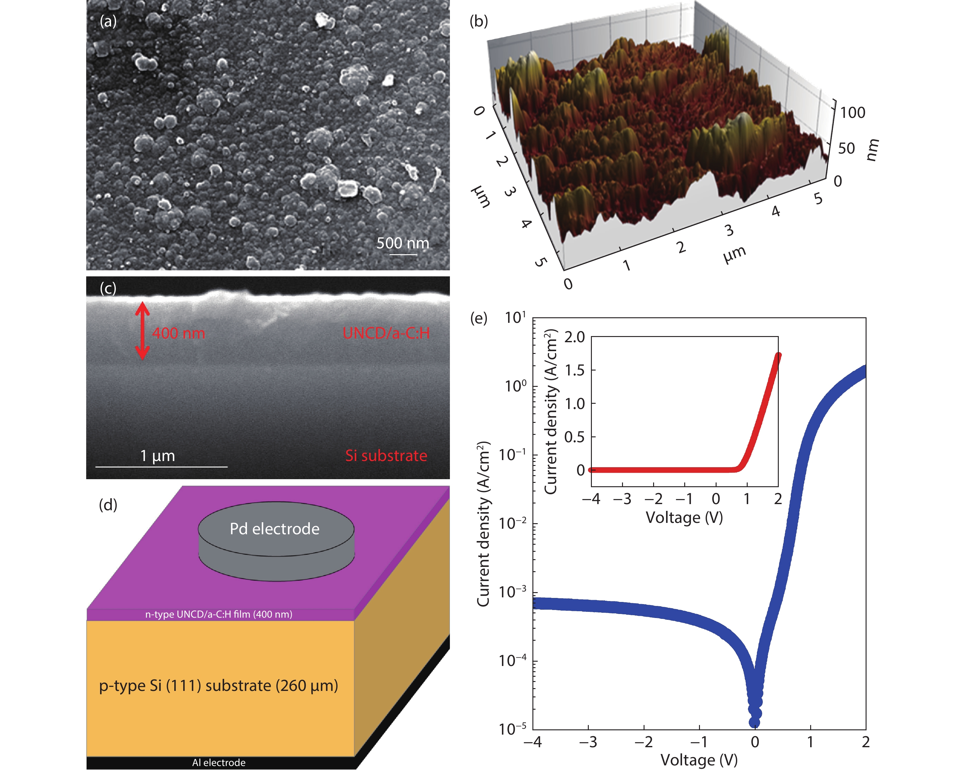
Fig. 1(a) illustrates the FESEM top-view image of UNCD/a-C:H film, deposited by the CAPD method. The formed N2-doped UNCD/a-C:H films comprise an enormous number of dissimilar nano-sized UNCD crystals surrounded by the a-C:H matrix. UNCD/a-C:H films, produced by CAPD and their surface morphology examined by AFM, typically demonstrate smooth surfaces. As shown in Fig. 1(b), the film surface roughness is within 100 nm with root-mean-square (rms) of 9–12 nm. These values are somewhat larger than those observed for undoped UNCD/a-C:H films (rms: 8 nm). As illustrated in Fig. 1(c), the cross-sectional FESEM image clearly illustrates a sharp film/substrate interface. This property is essential to accomplish heterojunction devices with good electric performance. Fig. 1(d) depicts a schematic representation of the fabricated (UNCD/a-C:H)/Si device with a film thickness of 400 nm and p-type Si(111) substrate thickness of 260 μm. Circular-shaped Pd ohmic contacts were formed on the film top surface, while Al ohmic contact was formed on the backside of the substrate. The diameter of the Pd electrode is 0.7 mm and the device effective device area is 3.8 × 10⁻³ cm2. Fig. 1(e) and (inset) show typical J–V characteristics of N2-doped UNCD/a-C:H film deposited on the Si substrate. The characteristics display noticeable rectifying action with a rectification ratio of more than three orders of magnitude at forward and reverse voltages of ± 2 V. This result confirms that the N2-doped UNCD/a-C:H films possess n-type conduction and a formulae pn heterojunction diode with the p-type Si substrate. The turn-on voltage of the junction, extracted from the linear plot of the forward bias J–V characteristics, was approximately 0.75 V. In the reverse bias direction, the leakage current density was 0.7 mA/cm2 at a reverse bias of –4 V. This current leakage might be attributed to thermally activated generation-recombination processes of charge carriers. Due to the presence of a considerable number of defects and charge-trapping centers in the UNCD/a-C:H film in addition to the existence of trap states at the film/substrate interface, the generation-recombination processes predominantly occur in the bulk and surface of the film.
![]()
Figure 1.(Color online) (a) Top-view FESEM images, (b) AFM image of UNCD/a-C:H film surface, (c) cross-sectional FESEM image, (d) schematic representation, and (e) semi-logarithmic and linear (inset)
Fig. 2 demonstrates frequency-dependent C–V characteristics of the N2-doped (UNCD/a-C:H)/p-Si device. The measured capacitance exhibited a strong dependence on both the applied DC bias voltage and the AC signal frequency. This dependence reveals the existence of a considerable number of defects and localized electronic states in both the UNCD/a-C:H film and the (n-UNCD/a-C:H)/p-Si interface. The capacitance increases with increasing the forward bias voltage, while it strongly decreases with increasing the reverse bias voltage. This can be referred to as diffusion and depletion capacitances commonly observed in conventional pn junctions. Under forward bias, the diffusion capacitance dominates and rises with increasing the applied voltage, as it is proportional to the forward current. On the other hand, the depletion capacitance dominates at reverse bias and decays with increasing the reverse bias voltage due to expanding the depletion-layer width. The capacitance also decreases with increasing of the signal frequency. At lower frequencies, the defect states can easily track the AC signal causing excessive capacitance values. At higher frequencies (greater than 100 kHz), the defect states cannot effectively follow the signal frequencies. This action degrades the contribution of the trap states to the total device capacitance measured for each bias voltage. The depletion-layer capacitance (C) is interrelated to the DC bias voltage (V) using the Schottky–Mott equation[
![]()
Figure 2.(Color online)
where q is the electric charge, A is the device area, ε1 and ε2 are the local permittivities, and
where W1 and W2 denote the depletion-region extensions inside the UNCD/a-C:H film and that of the Si substrate, respectively. The heterojunction built-in potential (Vbi) was directly extracted from 1/C2–V plots to be 0.75 V, as shown in Fig. 3. The latter values are consistent with that of the turn-on voltage (0.75 V) deduced from the linear plot of the heterojunction J–V characteristics, shown in Fig. 1(e). The 1/C2–V plots exhibited linear dependence of the applied voltage, demonstrating a homogeneous distribution of donor atoms in the depletion layer. The total width of the depletion-layer (W = W1 + W2) was extracted to be 322 nm and the doping concentration of the UNCD/a-C:H film was determined to be 1.95 × 1016 cm–3.
![]()
Figure 3.
The complex impedance (Z*) spectroscopy of the heterojunctions was measured in the temperature range of 300–400 K. Z* is commonly expressed as the vector summation of two parts: real (Zr) and imaginary (Zim) impedances. Figs. 4(a) and 4(b) show the temperature-dependent spectra of Zr and Zim. In this regard, Zr exhibited strong decay with increasing frequency and temperature. This impedance is attributed to carrier transportation resistance in UNCD/a-C:H film in addition to carrier recombination at film/electrode and film/substrate interfaces. Moreover, this resistance arises due to space-charge, dipoles, and electrons polarization in the film and Si substrate. At high frequencies, the polarized charges unable to follow fast changes of the AC signal, thus their influences on the impedance decline gradually with increasing frequency. Furthermore, Zr decreased with rising of the temperature due to carrier thermal generation from defects in UNCD/a-C:H film. On the other hand, Zim showed broadening peaks centered at frequencies above 105 Hz. The observed Zim peaks were slightly shifted to higher frequencies at increased temperatures. The signal angular-frequency (ω = 2πf) at which Zim is maximized can be related to relaxation time constant (τ) using the relation: ωmτ = 1. The time constant for thermal-emission of electrons from a trap state can be computed by[
![]()
Figure 4.(Color online)
where σn is the capture cross-section, vth is the thermal velocity, NC is the DOS in the conduction band, Ea is the activation energy of the trap states with respect to the conduction band edge, K is the Boltzmann constant, and T the temperature. The term σnνthNC defines what is called the attempt-to-escape-frequency (υ0)[
![]()
Figure 5.(Color online)
Fig. 6 depicts the Arrhenius plot of the extracted values of fm for each measured temperature. At high temperatures, more carriers are emitted from the traps excited by dissipated thermal energy in the UNCD/a-C:H film. Furthermore, as the temperature increases, fm increases, subsequently the trap response time becomes shorter. The characteristics frequency, υ0, was extracted to be 5.7 × 10⁵ Hz using linear fitting to the Arrhenius equation:
![]()
Figure 6.Arrhenius plot of ln(
The activation energy attained from the slope of the linear fit in the plot was determined to be 46 meV. This value is comparable with those obtained for the N2-doped UNCD films prepared with dissimilar deposition methods[
The trap states frequency response is regularly described in terms of a demarcation energy Ef, where this frequency-dependent energy is defined by[
Hence, the trap density-of-states (Nt) is computed by[
The energy distribution of a defect/trap state at an energy Ef can be evaluated by calculating the first derivative of the measured heterojunction capacitance with respect to the signal frequency.
Figs. 7(a)–7(e) show defect energy-distributed DOS deduced from Eqs. (6) and (7) using measured C–f characteristics of n-type UNCD/a-C:H films/p-type Si substrate, examined at different temperatures. Despite the noise that appeared in the derived DOS data, resulting from slight inaccuracy of the measuring instrument, particularly at high frequencies, in addition to the dispersion of the capacitance–frequency derivative (dC/df), fitting of the data showed nice consistency with the Gaussian equation:
![]()
Figure 7.Energy-distributed trap-DOS of N2-doped UNCD/a-C:H film measured (dots) and fitted (lines) data at temperatures of (a) 300 K, (b) 325 K, (c) 350 K, (d) 375 K, and (e) 400 K.
where NG is the DOS peak located at an energy E equals to that of a trap energy Et and σ denotes characteristic energy of the trap center. At room temperature, the Gaussian peak of 2.8 × 1016 cm–3eV–1 located at trap energy of 0.120 eV, with a characteristic energy of 0.064 eV, was deduced. These results are in good agreement with those obtained using J–V characterization[
Since nitrogen atoms preferentially integrate into GBs rather than into the UNCD grains, they tend to create additional conduction pathways in the films, causing the increase of electric conductivity of the films due to a significant increase in sp2-C and π-bonds in the composite. Therefore, the defect states are localized mainly in GBs in the UNCD/a-C:H films. The bulk defects, in addition to the interface defects, might be the main causes of the leakage current observed in (n-type UNCD/a-C:H)/p-type Si heterojunction devices. Suppression of these defects can be attainable through the optimization of the inflow-rate ratio of N2/H2 mixed-gases introduced during the film perpetration. This investigation is to be reported elsewhere.
4. Conclusions
Thin films comprising N2-doped UNCD/a-C:H composite films, were experimentally investigated. The films, deposited on p-type Si substrates by the CAPD method, were characterized by C–f measured in the temperature and frequency ranges of 300–400 K and 50 kHz–2 MHz, respectively. In the measured temperature range, the traps exhibited Gaussian-distributed states with peak values lying in the range: 2.84 × 10¹⁶–2.73 × 10¹⁷ eV–1cm–3. The characteristics energies of these states were in the range of 50–64 meV. At 300 K, the trap centered at 120 meV below the conduction band and shifted to 233 meV when the temperature raised to 400 K. These states are generated due to a large amount of sp2-C and π-bond states, localized in GBs of the UNCD/a-C:H film. By optimizing the inflow-rate ratio of N2/H2 mixed-gases introduced during plasma deposition, suppression of these defects can be achieved.
Acknowledgements
The author appreciates Professor Tsuyoshi Yoshitake and Dr. Abdelrahman Zkria, at Yoshitake Laboratory, Department of Applied Science of Electronics and Materials, Interdisciplinary Graduate School of Engineering Sciences, Kyushu University, Fukuoka, Japan, for providing very helpful information on experimental investigations of the N2-doped UNCD/a-C:H composite.
References
[1]
[2] P W May. Diamond thin films: A 21st-century material. Philos Trans Royal Soc Lond Ser A, 358, 473(2000).
[3] S C Mi, M Kiss, T Graziosi et al. Integrated photonic devices in single crystal diamond. J Phys Photonics, 2, 042001(2020).
[4] A Kobayashi, S Ohmagari, H Umezawa et al. Suppression of killer defects in diamond vertical-type Schottky barrier diodes. Jpn J Appl Phys, 59, SGGD10(2020).
[5] T Matsumoto, H Kato, K Oyama et al. Inversion channel diamond metal-oxide-semiconductor field-effect transistor with normally off characteristics. Sci Rep, 6, 31585(2016).
[6] X Y Peng, Y M Li, S K Duan et al. Precise ultrananocrystalline diamond nanowire arrays for high performance gas sensing application. Mater Lett, 265, 127404(2020).
[7] S Jiao, A Sumant, M A Kirk et al. Microstructure of ultrananocrystalline diamond films grown by microwave Ar–CH4 plasma chemical vapor deposition with or without added H2. J Appl Phys, 90, 118(2001).
[8] M Bevilacqua, N Tumilty, C Mitra et al. Nanocrystalline diamond as an electronic material: An impedance spectroscopic and Hall effect measurement study. J Appl Phys, 107, 033716(2010).
[9] O Auciello, A V Sumant. Status review of the science and technology of ultrananocrystalline diamond (UNCD™) films and application to multifunctional devices. Diam Relat Mater, 19, 699(2010).
[10] H J Zeng, A R Konicek, N Moldovan et al. Boron-doped ultrananocrystalline diamond synthesized with an H-rich/Ar-lean gas system. Carbon, 84, 103(2015).
[11] M Mertens, M Mohr, N Wiora et al. N-type conductive ultrananocrystalline diamond films grown by hot filament CVD. J Nanomater, 2015, 1(2015).
[12] T Ikeda, K Teii, C Casiraghi et al. Effect of the sp2 carbon phase on n-type conduction in nanodiamond films. J Appl Phys, 104, 073720(2008).
[13] P Zapol, M Sternberg, L A Curtiss et al. Tight-binding molecular-dynamics simulation of impurities in ultrananocrystalline diamond grain boundaries. Phys Rev B, 65, 045403(2001).
[14] S Bhattacharyya, O Auciello, J Birrell et al. Synthesis and characterization of highly-conducting nitrogen-doped ultrananocrystalline diamond films. Appl Phys Lett, 79, 1441(2001).
[15] J Birrell, J E Gerbi, O Auciello et al. Bonding structure in nitrogen doped ultrananocrystalline diamond. J Appl Phys, 93, 5606(2003).
[16] W Kulisch, C Popov, E Lefterova et al. Electrical properties of ultrananocrystalline diamond/amorphous carbon nanocomposite films. Diam Relat Mater, 19, 449(2010).
[17] A Voss, S R Stateva, J P Reithmaier et al. Patterning of the surface termination of ultrananocrystalline diamond films for guided cell attachment and growth. Surf Coat Technol, 321, 229(2017).
[18] K Hanada, T Nishiyama, T Yoshitake et al. Optical emission spectroscopy of deposition process of ultrananocrystalline diamond/hydrogenated amorphous carbon composite films by using a coaxial arc plasma gun. Diam Relat Mater, 19, 899(2010).
[19] R Chaleawpong, N Promros, A Zkria et al. Diode parameters and ultraviolet light detection characteristics of n-type silicon/p-type nanocrystalline diamond heterojunctions at different temperatures. Thin Solid Films, 709, 138222(2020).
[20] A M Ali, T Deckert-Gaudig, M Egiza et al. Near- and far-field Raman spectroscopic studies of nanodiamond composite films deposited by coaxial arc plasma. Appl Phys Lett, 116, 041601(2020).
[21] Y Katamune, S Al-Riyami, S Takeichi et al. Study on defects in ultrananocrystalline diamond/amorphous carbon composite films prepared by physical vapor deposition. ECS Trans, 75, 45(2017).
[22] A Zkria, E Abubakr, P Sittimart et al. Analysis of electrical characteristics of Pd/n-nanocarbon/p-Si heterojunction diodes: By CVf and G/wVf. J Nanomater, 2020, 4917946(2020).
[23] A Zkria, F Abdel-Wahab, Y Katamune et al. Optical and structural characterization of ultrananocrystalline diamond/hydrogenated amorphous carbon composite films deposited via coaxial arc plasma. Curr Appl Phys, 19, 143(2019).
[24] S Al-Riyami, S Ohmagari, T Yoshitake. Nitrogen-doped ultrananocrystalline diamond/hydrogenated amorphous carbon composite films prepared by pulsed laser deposition. Appl Phys Express, 3, 115102(2010).
[25] A Zkria, H Gima, M Shaban et al. Electrical characteristics of nitrogen-doped ultrananocrystalline diamond/hydrogenated amorphous carbon composite films prepared by coaxial arc plasma deposition. Appl Phys Express, 8, 095101(2015).
[26] H Gima, A Zkria, Y Katamune et al. Chemical bonding structural analysis of nitrogen-doped ultrananocrystalline diamond/hydrogenated amorphous carbon composite films prepared by coaxial arc plasma deposition. Appl Phys Express, 10, 015801(2017).
[27] A Zkria, M Shaban, T Hanada et al. Current transport mechanisms in N-type ultrananocrystalline diamond/p-type Si heterojunctions. J Nanosci Nanotechnol, 16, 12749(2016).
[28] A Zkria, H Gima, T Yoshitake. Application of nitrogen-doped ultrananocrystalline diamond/hydrogenated amorphous carbon composite films for ultraviolet detection. Appl Phys A, 123, 167(2017).
[29] A Zkria, T Yoshitake. Temperature-dependent current–voltage characteristics and ultraviolet light detection of heterojunction diodes comprising n-type ultrananocrystalline diamond/hydrogenated amorphous carbon composite films and p-type silicon substrates. Jpn J Appl Phys, 56, 07KD04(2017).
[30] M Shaban, A Zkria, T Yoshitake. Characterization and design optimization of heterojunction photodiodes comprising n-type ultrananocrystalline diamond/hydrogenated amorphous carbon composite and p-type Si. Mater Sci Semicond Process, 86, 115(2018).
[31] A Zkria, M Shaban, E Abubakr et al. Impedance spectroscopy analysis of n-type (nitrogen-doped) ultrananocrystalline diamond/p-type Si heterojunction diodes. Phys Scr, 95, 095803(2020).
[32] M Shaban. Modeling, design, and simulation of Schottky diodes based on ultrananocrystalline diamond composite films. Semicond Sci Technol, 36, 015004(2020).
[33]
[34]
[35] J A Carr, M Elshobaki, S Chaudhary. Deep defects and the attempt to escape frequency in organic photovoltaic materials. Appl Phys Lett, 107, 203302(2015).
[36] T Makino, H Kato, S G Ri et al. Electrical characterization of homoepitaxial diamond p-n+ junction. Diam Relat Mater, 14, 1995(2005).
[37] X F Zhang, T Matsumoto, U Sakurai et al. Energy distribution of Al2O3/diamond interface states characterized by high temperature capacitance-voltage method. Carbon, 168, 659(2020).
[38] H Xu, H T Ye, D Coathup et al. An insight of p-type to n-type conductivity conversion in oxygen ion-implanted ultrananocrystalline diamond films by impedance spectroscopy. Appl Phys Lett, 110, 033102(2017).
[39] V D Frolov, S M Pimenov, V I Konov et al. Electronic properties of low-field-emitting ultrananocrystalline diamond films. Surf Interface Anal, 36, 449(2004).
[40] N Wiora, M Mertens, K Brühne et al. Grain boundary dominated electrical conductivity in ultrananocrystalline diamond. J Appl Phys, 122, 145102(2017).
[41] T Walter, R Herberholz, C Muller et al. Determination of defect distributions from admittance measurements and application to Cu(In, Ga)Se2 based heterojunctions. J Appl Phys, 80, 4411(1996).


Set citation alerts for the article
Please enter your email address

© Copyright 2018-2021 | Chinese Laser Press. All Rights Reserved 沪ICP备15018463号-20