
Lan Bi, Yixu Yao, Qimeng Jiang, Sen Huang, Xinhua Wang, Hao Jin, Xinyue Dai, Zhengyuan Xu, Jie Fan, Haibo Yin, Ke Wei, Xinyu Liu. Instability of parasitic capacitance in T-shape-gate enhancement-mode AlGaN/GaN MIS-HEMTs[J]. Journal of Semiconductors, 2022, 43(3): 032801
- Journal of Semiconductors
- Vol. 43, Issue 3, 032801 (2022)
Abstract
1. Introduction
AlGaN/GaN high-electron mobility transistors (HEMTs) or metal–insulator–semiconductor HEMTs (MIS-HEMTs), by virtue of the superior polarization-induced high mobility 2-D electron gas (2DEG), are well-proposed for their high switching speed, low parasitic parameters and low on-resistance, and have achieved recognized success in both high frequency RF and power switching applications[
In this work, gate-related parasitic capacitances of the T-shape-gate E-mode AlGaN/GaN HEMT were investigated by high-frequency C–V measurements as well as the inductive switching measurement, where CGD was individually observed during the Miller plateau. The instability of CGD, caused by the trapping/de-trapping of deep interface/bulk states in LPCVD-SiNx dielectric in the gate overhang region[
2. Device fabrication and characteristics of E-mode MIS-HEMT
The E-mode MIS-HEMT was fabricated on an ultra-thin-barrier (UTB) AlGaN/GaN heterostructure grown on the Si substrate[
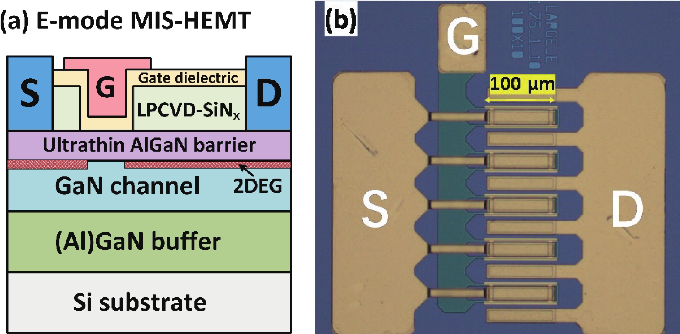
![]()
Figure 1.(Color online) (a) Cross sectional schematic of the E-mode AlGaN/GaN MIS-HEMT. (b) Microscope photograph of a 1-mm device.
Fig. 2(a) shows the transfer characteristics at drain bias VDS = 1 V and VDS = 10 V. The E-mode MIS-HEMT exhibits a threshold voltage VTH of 1.26 V defined at ID = 1 μA with a hysteresis of 0.3 V at VDS = 1 V, indicating a decent ALD-SiNx/AlGaN (F-etched) interface quantity. Fig. 2(b) shows the output characteristics. A saturation current of 339 mA is obtained at VGS = 8 V. Fig. 2(c) shows the three-terminal off-state currents at VGS = 0 V. A small drain leakage lower than 10–6 mA is obtained and the gate leakage is always around 10 times lower.
![]()
Figure 2.(Color online) (a) Transfer, (b) output, and (c) three-terminal off-state leakage of the 1-mm E-mode MIS-HEMT.
3. Gate-related capacitances and dynamic characteristics of E-mode MIS-HEMT
Fig. 3(a) shows the schematic of the gate-related capacitances in the T-shape gate E-mode AlGaN/GaN MIS-HEMT. C2 is the channel capacitance performing in the E mode and C1/C3 is the gate-source/drain overlay capacitance performing in the depletion mode (D mode). Multi-frequency C–V measurements were conducted on the T-shape gate E-mode MIS-HEMT with source and drain both grounded (shown in Fig. 3(b)), and the CG–VG curves are shown in Fig. 3(c). Two pinch-off points are observed in the whole VG range, corresponding to different capacitance components. The first one at VG ~ –10 V is related to the overhang capacitances (i.e., C1 and C3), and the second one is related to the E-mode channel (i.e., C2). Very small frequency dispersion is observed on both E-mode gate and D-mode gate overhang, informing a high quality ALD-SiNx/(Al)GaN and LPCVD-SiNx/(Al)GaN interface. Unlike the E-mode portion, the D-mode portion exhibits a noticeable hysteresis between up- and down-sweeping curve, probably caused by deep interface/bulk states in the LPCVD-SiNx passivation dielectric.
![]()
Figure 3.(Color online) (a) Schematic of the gate-related capacitances in T-shape gate E-mode AlGaN/GaN MIS-HEMT. (b) Bias set of the
Since the Miller capacitance CGD plays an important role on the device switching performance, in this paper, CGD was individually investigated by C–V measurement with a shorted source/gate terminal and a sweeping drain terminal, as shown in Fig. 4(a). In this measurement, drain terminal voltage (VDG) is swept from an initial voltage Vinit (holding for 30 seconds before C–V sweep) to 25 V and double-mode sweep was used to estimate the instability of the CGD. It is noted that a negative VDG, corresponding to a positive bias applied on the overhang capacitor, is able to assist the spill-over of the electrons to the SiNx/(Al)GaN interface as well as the trapping of the interface or dielectric bulk states. Fig. 4(b) plots the measurement results and an obvious hysteresis (> 1.5 V) on the up- and down-sweep D-mode pinch-off voltage is obtained, which is directly dependent on the magnitude of the negative stress voltageVinit. The hysteresis increases owing to the enhanced trapping in the passivation dielectric. In the down-sweep curves under different initial stress, the D-mode pinch-off voltage merges together, indicating that an efficient electrons’ de-trapping is achieved with a 25 V VDG.
![]()
Figure 4.(Color online) (a) Bias set of the
In this work, to further identify the effect of the overhang capacitance on the device switching performance, a double-pulse measurement was executed with measurement setup plotted in Fig. 5(a). A device bare die was mounted on a testing PCB by conductive silver epoxy, and its pads were bonded out by golden wires. A simple gate driver circuit is used with a separate turn-on and turn-off path. In order to enlarge the Miller plateau, a 10 kΩ charging resistor was used to slow down the turning-on process. The waveform of inductive switching under 50 V VBUS and the turn-on transients are shown in Figs. 5(b) and 5(c). During the turn-on period of the second pulse, the presence of the D-mode portion of CGD reduces the slew rate of output voltage, leading to a longer Miller plateau and extra switching power loss. The turning point of two sections of dVDS/dt is around 10 V in the beginning of Miller plateau, which coincides with the pinch-off voltage of CGD.
![]()
Figure 5.(Color online) (a) Schematic and photo of the inductive switching circuit. (b) Waveform of the inductive switching under 50-V
4. Conclusion
In this work, gate-related capacitances of the T-shape-gate E-mode AlGaN/GaN HEMT have been investigated by C–V measurements and the inductive switching measurement. The overhang-related CGD exhibits a noticeable hysteresis in double sweeps, informing its sensitivity to forward stressing voltage due to the trapping of deep interface/bulk states of LPCVD-SiNx passivation dielectrics. During the turn-on period of inductive switching measurement, two sections of dVDS/dt with a turning point around 10 V are observed for the presence of D-mode portion in CGD, leading to a longer switching transfer and higher switching power loss.
Acknowledgements
This work was supported in part by the National Natural Science Foundation of China under Grant 61822407, Grant 61527816, Grant 11634002, Grant 61631021, Grant 62074161, Grant 62004213, and Grant U20A20208; in part by the Key Research Program of Frontier Sciences, Chinese Academy of Sciences (CAS) under Grant QYZDB-SSW-JSC012; in part by the Youth Innovation Promotion Association of CAS; in part by the University of CAS; and in part by the Opening Project of Key Laboratory of Microelectronic Devices & Integrated Technology, Institute of Microelectronics, CAS.
References
[1] K S Boutros, R M Chu, B Hughes. GaN power electronics for automotive application. 2012 IEEE Energytech, 1(2012).
[2] D Piedra, B Lu, M Sun et al. Advanced power electronic devices based on gallium nitride (GaN). 2015 IEEE International Electron Devices Meeting, 16.6.1(2015).
[3] I C Kizilyalli, Y A Xu, E Carlson et al. Current and future directions in power electronic devices and circuits based on wide band-gap semiconductors. 2017 IEEE 5th Work Wide Bandgap Power Devices Appl, 417(2017).
[4] K J Chen, O Häberlen, A Lidow et al. GaN-on-Si power technology: Devices and applications. IEEE Trans Electron Devices, 64, 779(2017).
[5] W Saito, T Nitta, Y Kakiuchi et al. Suppression of dynamic on-resistance increase and gate charge measurements in high-voltage GaN-HEMTs with optimized field-plate structure. IEEE Trans Electron Devices, 54, 1825(2007).
[6] R M Chu, A Corrion, M Chen et al. 1200-V normally off GaN-on-Si field-effect transistors with low dynamic on -resistance. IEEE Electron Device Lett, 32, 632(2011).
[7] X B Ma, J C Zhang, L L Guo et al. Effects of passivation and FP structure on current collapse in an AlGaN/GaN HEMT. Chin J Semicond, 28, 73(2007).
[8] Y Lei, u H Lu. Influence of field plate on surface-state-related lag characteristics of AlGaN/GaN HEMT. J Semicond, 36, 074007(2015).
[9] G Meneghesso, D Bisi, I Rossetto et al. Reliability of power devices: Bias-induced threshold voltage instability and dielectric breakdown in GaN MIS-HEMTs. 2016 IEEE Int Integr Reliab Work, 35(2016).
[10] R Zhao, S Huang, X H Wang et al. Interface charge engineering in down-scaled AlGaN (<6 nm)/GaN heterostructure for fabrication of GaN-based power HEMTs and MIS-HEMTs. Appl Phys Lett, 116, 103502(2020).
[11] S Yang, Z K Tang, M Y Hua et al. Investigation of SiN
[12] A G Viey, W Vandendaele, M A Jaud et al. Investigation of nBTI degradation on GaN-on-Si E-mode MOSc-HEMT. 2019 IEEE International Electron Devices Meeting, 4.3.1(2019).
[13] S Huang, X Liu, X Wang et al. Ultrathin-barrier AlGaN/GaN heterostructure: a recess-free technology for manufacturing high-performance GaN-on-Si power devices. IEEE Trans on Electron Devices, 65, 207(2018).
[14] S Huang, X H Wang, X Y Liu et al. Monolithic integration of E/D-mode GaN MIS-HEMTs on ultrathin-barrier AlGaN/GaN heterostructure on Si substrates. Appl Phys Express, 12, 024001(2019).
[15] S Huang, X Y Liu, X H Wang et al. High uniformity normally-OFF GaN MIS-HEMTs fabricated on ultra-thin-barrier AlGaN/GaN heterostructure. IEEE Electron Device Lett, 37, 1617(2016).
[16] F Q Guo, S Huang, X H Wang et al. Suppression of interface states between nitride-based gate dielectrics and ultrathin-barrier AlGaN/GaN heterostructure with


Set citation alerts for the article
Please enter your email address

© Copyright 2018-2021 | Chinese Laser Press. All Rights Reserved 沪ICP备15018463号-20