• Journal of Semiconductors
  • Vol. 43, Issue 12, 122802 (2022)
Xiaojie Wang1, Zhanwei Shen2、*, Guoliang Zhang1, Yuyang Miao1, Tiange Li1, Xiaogang Zhu1, Jiafa Cai1, Rongdun Hong1、3, Xiaping Chen1, Dingqu Lin1, Shaoxiong Wu1, Yuning Zhang1, Deyi Fu1, Zhengyun Wu1, and Feng Zhang1、4、**
Author Affiliations
  • 1College of Physical Science and Technology, Xiamen University, Xiamen 361005, China
  • 2Key Laboratory of Semiconductor Material Sciences, Institute of Semiconductors, Chinese Academy of Sciences, Beijing 100083, China
  • 3Shenzhen Research Institute of Xiamen University, Shenzhen 518057, China
  • 4Jiujiang Research Institute of Xiamen University, Jiujiang 332000, China
  • show less
    DOI: 10.1088/1674-4926/43/12/122802 Cite this Article
    Xiaojie Wang, Zhanwei Shen, Guoliang Zhang, Yuyang Miao, Tiange Li, Xiaogang Zhu, Jiafa Cai, Rongdun Hong, Xiaping Chen, Dingqu Lin, Shaoxiong Wu, Yuning Zhang, Deyi Fu, Zhengyun Wu, Feng Zhang. A 4H-SiC semi-super-junction shielded trench MOSFET: p-pillar is grounded to optimize the electric field characteristics[J]. Journal of Semiconductors, 2022, 43(12): 122802 Copy Citation Text show less
    (Color online) Schematic cross-sections of (a) the CT-UMOS and (b) proposed SS-UMOS (G & NG) (Please refer to Table 1 for detailed parameters).
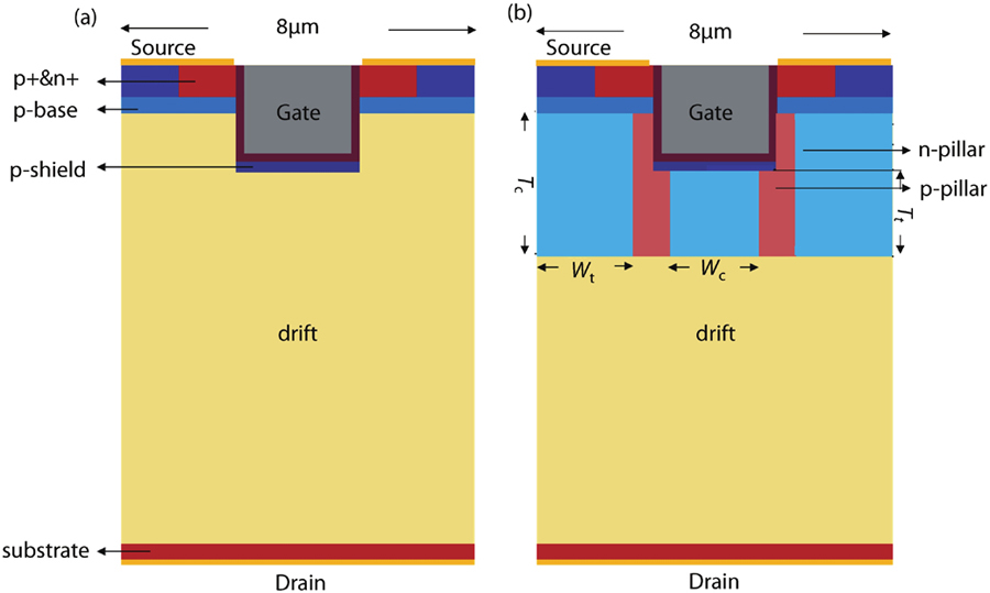
    Fig. 1. (Color online) Schematic cross-sections of (a) the CT-UMOS and (b) proposed SS-UMOS (G & NG) (Please refer to Table 1 for detailed parameters).
    (Color online) Process flow of the proposed SS-UMOS (G & NG) structure of SiC MOSFET.
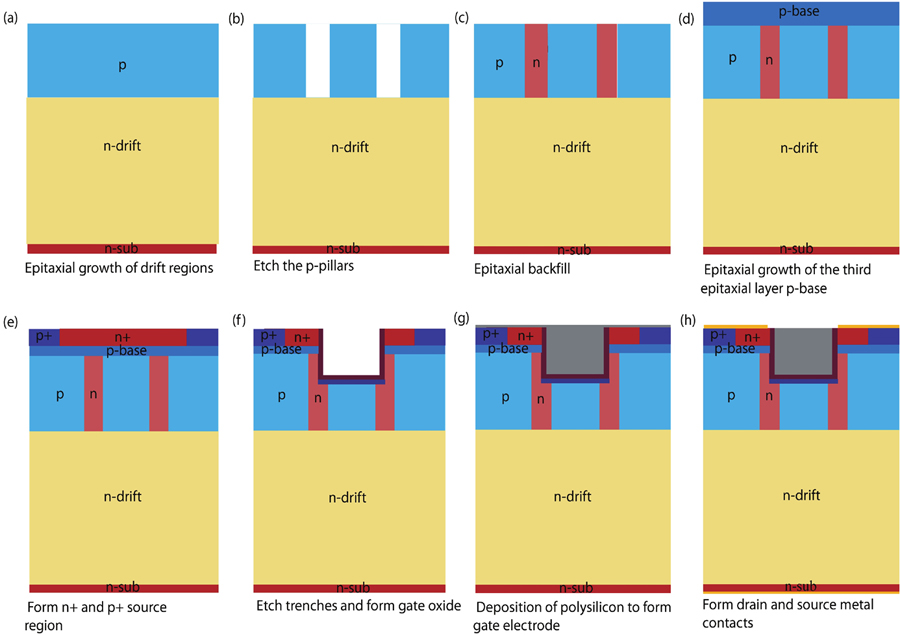
    Fig. 2. (Color online) Process flow of the proposed SS-UMOS (G & NG) structure of SiC MOSFET.
    (Color online) (a) The transfer characteristic curves (VDS = 5 V), (b) output characteristic curves and current density of (c) CT-UMOS, (d) GSS-UMOS, (e) NGSS-UMOS. (VGS = 15 V,VDS = 20 V)
    Fig. 3. (Color online) (a) The transfer characteristic curves (VDS = 5 V), (b) output characteristic curves and current density of (c) CT-UMOS, (d) GSS-UMOS, (e) NGSS-UMOS. (VGS = 15 V,VDS = 20 V)
    (Color online) (a) Breakdown characteristic curves, (b–d) corresponding electric field distributions (VGS = 0 V,VDS = 1200 V), two-dimensional electric fields of (e) CT-UMOS and (f) GSS-UMOS (VGS = 0 V,VDS = 1200 V), and current density distribution of (g) CT-UMOS and (h) GSS-UMOS at breakdown voltage.
    Fig. 4. (Color online) (a) Breakdown characteristic curves, (b–d) corresponding electric field distributions (VGS = 0 V,VDS = 1200 V), two-dimensional electric fields of (e) CT-UMOS and (f) GSS-UMOS (VGS = 0 V,VDS = 1200 V), and current density distribution of (g) CT-UMOS and (h) GSS-UMOS at breakdown voltage.
    (Color online) (a) Feedback capacitance CGD as a function of drain voltageVDS at gate voltage VGS = 0 V and (b) voltage VGS as a function of gate chargeQG and the inset is the testing circuit forQG.
    Fig. 5. (Color online) (a) Feedback capacitance CGD as a function of drain voltageVDS at gate voltage VGS = 0 V and (b) voltage VGS as a function of gate chargeQG and the inset is the testing circuit forQG.
    (Color online) (a) Test circuit of switch characteristics, (b) voltage and current characteristic of the GSS-UMOS in the switching transients, (c) detailed comparisons of the turn-on and turn-off transients for the CT-UMOS and SS-UMOS (G & NG) at switching frequency of 33 kHz, (d) the switching frequency is 50 kHz, (e) the switching frequency is 75 kHz, (f) comparison of the switching loss at different switching frequencies.
    Fig. 6. (Color online) (a) Test circuit of switch characteristics, (b) voltage and current characteristic of the GSS-UMOS in the switching transients, (c) detailed comparisons of the turn-on and turn-off transients for the CT-UMOS and SS-UMOS (G & NG) at switching frequency of 33 kHz, (d) the switching frequency is 50 kHz, (e) the switching frequency is 75 kHz, (f) comparison of the switching loss at different switching frequencies.
    (Color online) The relationship between the total power loss and switching frequency.
    Fig. 7. (Color online) The relationship between the total power loss and switching frequency.
    Device parameterCT-UMOSSS-UMOS
    p-body junction depth (μm)0.50.5
    p+ junction depth (μm)0.20.2
    Gate trench depth (μm)1.81.8
    Thickness of n-drift (μm)1212
    n-pillar depth (Tt) (μm)1.5
    p-pillar depth (Tt) (μm)1.5
    n-pillar depth (Tc) (μm)2.8
    p-pillar depth (Tc) (μm)2.8
    p-pillar width (Wc) (μm)2.2
    p-pillar width (Wt) (μm)1.6
    Width of trench (μm)2.02.0
    n-drift doping concentration (1015 cm−3)1.01.0
    p-body doping concentration (1017 cm−3)1.01.0
    p-pillar doping concentration (1016 cm−3)3.0
    n-pillar doping concentration (1016 cm−3)2.0
    Table 0. Device parameters for CT-UMOS and SS-UMOS (G & NG).
    ParameterCT-UMOSGSS-UMOSNGSS-UMOSr
    Isat (kA/cm2)2.403.906.70
    Ron,sp (mΩ·cm2)6.203.001.80
    BV (V)124017501530
    Eox-max (MV/cm)3.002.202.70
    Eox (MV/cm)1.501.002.70
    Etotal (mJ/cm2)2.401.95
    FOM (kV2/(mΩ·cm2))0.260.901.30
    QGD (nC/cm2)24580450
    QG (nC/cm2)302829222980
    Ciss (nF/cm2)6730 108
    QGD·Ron,sp (mΩ·nC)1550240810
    Table 0. Comparisons of the characteristics for the CT-UMOS and the SS-UMOS (G & NG).
    Xiaojie Wang, Zhanwei Shen, Guoliang Zhang, Yuyang Miao, Tiange Li, Xiaogang Zhu, Jiafa Cai, Rongdun Hong, Xiaping Chen, Dingqu Lin, Shaoxiong Wu, Yuning Zhang, Deyi Fu, Zhengyun Wu, Feng Zhang. A 4H-SiC semi-super-junction shielded trench MOSFET: p-pillar is grounded to optimize the electric field characteristics[J]. Journal of Semiconductors, 2022, 43(12): 122802
    Download Citation