Abstract
A 4H-SiC trench gate metal–oxide–semiconductor field-effect transistor (UMOSFET) with semi-super-junction shielded structure (SS-UMOS) is proposed and compared with conventional trench MOSFET (CT-UMOS) in this work. The advantage of the proposed structure is given by comprehensive study of the mechanism of the local semi-super-junction structure at the bottom of the trench MOSFET. In particular, the influence of the bias condition of the p-pillar at the bottom of the trench on the static and dynamic performances of the device is compared and revealed. The on-resistance of SS-UMOS with grounded (G) and ungrounded (NG) p-pillar is reduced by 52% (G) and 71% (NG) compared to CT-UMOS, respectively. Additionally, gate oxide in the GSS-UMOS is fully protected by the p-shield layer as well as semi-super-junction structure under the trench and p-base regions. Thus, a reduced electric-field of 2 MV/cm can be achieved at the corner of the p-shield layer. However, the quasi-intrinsic protective layer cannot be formed in NGSS-UMOS due to the charge storage effect in the floating p-pillar, resulting in a large electric field of 2.7 MV/cm at the gate oxide layer. Moreover, the total switching loss of GSS-UMOS is 1.95 mJ/cm2 and is reduced by 18% compared with CT-UMOS. On the contrary, the NGSS-UMOS has the slowest overall switching speed due to the weakened shielding effect of the p-pillar and the largest gate-to-drain capacitance among the three. The proposed GSS-UMOS plays an important role in high-voltage and high-frequency applications, and will provide a valuable idea for device design and circuit applications.A 4H-SiC trench gate metal–oxide–semiconductor field-effect transistor (UMOSFET) with semi-super-junction shielded structure (SS-UMOS) is proposed and compared with conventional trench MOSFET (CT-UMOS) in this work. The advantage of the proposed structure is given by comprehensive study of the mechanism of the local semi-super-junction structure at the bottom of the trench MOSFET. In particular, the influence of the bias condition of the p-pillar at the bottom of the trench on the static and dynamic performances of the device is compared and revealed. The on-resistance of SS-UMOS with grounded (G) and ungrounded (NG) p-pillar is reduced by 52% (G) and 71% (NG) compared to CT-UMOS, respectively. Additionally, gate oxide in the GSS-UMOS is fully protected by the p-shield layer as well as semi-super-junction structure under the trench and p-base regions. Thus, a reduced electric-field of 2 MV/cm can be achieved at the corner of the p-shield layer. However, the quasi-intrinsic protective layer cannot be formed in NGSS-UMOS due to the charge storage effect in the floating p-pillar, resulting in a large electric field of 2.7 MV/cm at the gate oxide layer. Moreover, the total switching loss of GSS-UMOS is 1.95 mJ/cm2 and is reduced by 18% compared with CT-UMOS. On the contrary, the NGSS-UMOS has the slowest overall switching speed due to the weakened shielding effect of the p-pillar and the largest gate-to-drain capacitance among the three. The proposed GSS-UMOS plays an important role in high-voltage and high-frequency applications, and will provide a valuable idea for device design and circuit applications.Introduction
| Device parameter | CT-UMOS | SS-UMOS |
|---|
| p-body junction depth (μm) | 0.5 | 0.5 |
| p+ junction depth (μm) | 0.2 | 0.2 |
| Gate trench depth (μm) | 1.8 | 1.8 |
| Thickness of n-drift (μm) | 12 | 12 |
| n-pillar depth (Tt) (μm) | – | 1.5 |
| p-pillar depth (Tt) (μm) | – | 1.5 |
| n-pillar depth (Tc) (μm) | – | 2.8 |
| p-pillar depth (Tc) (μm) | – | 2.8 |
| p-pillar width (Wc) (μm) | – | 2.2 |
| p-pillar width (Wt) (μm) | – | 1.6 |
| Width of trench (μm) | 2.0 | 2.0 |
| n-drift doping concentration (1015 cm−3) | 1.0 | 1.0 |
| p-body doping concentration (1017 cm−3) | 1.0 | 1.0 |
| p-pillar doping concentration (1016 cm−3) | – | 3.0 |
| n-pillar doping concentration (1016 cm−3) | – | 2.0 |
Table 0. Device parameters for CT-UMOS and SS-UMOS (G & NG).
As one of the representatives of the wide bandgap semiconductor materials, silicon carbide (SiC) has competitive advantages such as, high critical breakdown electric field, high thermal conductivity and high electron mobility compared with the traditional material of silicon (Si). In addition, the maturity of SiC technology makes it more and more recognizable and available for academia and industry. Therefore, SiC is one of the promising candidates to replace Si and is widely used in power semiconductor devices, such as metal–oxide–semiconductor field effect transistor (MOSFETs), insulated gate bipolar transistor (IGBTs), etc[1,2].
In particular, SiC MOSFETs have the characteristics of easy driving, high switching frequency, and low loss, enabling them show great advantages in new energy vehicles and charging facilities[3-5]. Power MOSFET includes two kinds of prototypes, namely vertical double-diffused MOSFET (VDMOSFET) and trench MOSFET (UMOSFET). It is attributed to the reason that SiC UMOSFET has the advantages of small cell and high channel mobility compared to the VDMOSFET. Accordingly, the investigation into SiC UMOSFET is gaining more and more attention in the power electronics field[6].
However, there are also many potential challenges, such as electric field accumulation at the corner of the trench, unreliability of the gate oxide layer, and instability of the threshold voltage[7,8], hindering their practical use for SiC UMOSFET. One of the critical issues is solved by adding a p-shield layer under the trench to reduce the maximum electric field (Eox-max) at the trench corner of the gate oxide. However, the p-shield brings the junction field effect transistor (JFET) effect, which increases the overall on-resistance of the device[9-13]. Generally, there is a trade-off between the on-resistance of the device and the electric field of the gate oxide. The reduction of the electric field of the gate oxide is at the expense of increasing the on-resistance or power loss of the device[14]. With regard to the switching losses, large miller capacitance (CGD) introduced by the gate-drain overlap has become the dominated challenge, affecting the high-frequency power consumptions in a single period interval. Therefore, a new work needs to be proposed to ensure that the device has lowCGD andEox-max, which can make the device separately attain low switching loss and high breakdown voltage. Herein, adding a super-junction structure to a trench MOSFET can alleviate the negative effects of the trench structure while maintaining the advantages of the trench structure. Thus, it achieves a superior trade-off between the static and dynamic performances of SiC trench MOSFET[15-24].
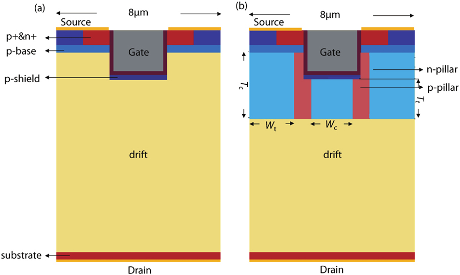
As shown inFig. 1, a semi-super-junction UMOSFET structure (SS-UMOS), with p-pillars and n-pillars added under the channels and trench regions, is proposed in this paper[25,26]. All the devices are simulated by TCAD. In addition to the comparison with CT-UMOS, this work also presents the effect of p-pillar’s bias conditions (grounded or ungrounded) on the electrical characteristics of SS-UMOS on the device. The detailed simulation parameters of the structure are listed inTable 1. The physical models of Shockley-Read-Hall, Auger, and incomplete dopants are involved in all structures. In addition, the 1 × 1012 cm–2 positive charge captured at the SiC–SiO2 interface is included in the devices[27-29]. The simulation results show that SS-UMOS has lower on-resistance, higher breakdown voltage and smaller switching losses compared with the conventional UMOSFETs (CT-UMOS). A discussion of possible manufacturing processes is described in detail. The parameters used in the simulation have been carefully optimized to achieve lowEox-max andRon,sp, and improve the dynamic performance of the device[29-31].

Figure 1.(Color online) Schematic cross-sections of (a) the CT-UMOS and (b) proposed SS-UMOS (G & NG) (Please refer to Table 1 for detailed parameters).
Structures and manufacturability
The manufacturability of the proposed SiC UMOSFET relies on advanced photolithographic and etching technique. Based on the process-related experiences obtained by other research groups[23,25,26], the primary analysis of the process flow is beneficial for the proposed device to achieve a manufacturable solution in the future.Fig. 2 shows a process flow of the proposed structure in this paper. It can be seen fromFig. 2(a) that the sandwich p–n epitaxial layers, from bottom to top, are epitaxially grown on the SiC substrate, which are the first epitaxial layer and the second epitaxial layer, with doping concentration of 1 × 10¹⁵ and 3 × 1016 cm–3, respectively. Next, periodically arranged trenches with depth of 2.8μm were etched with HF in the p-pillar, as shown inFig. 2(b). Then, as shown inFig. 2(c), epitaxial backfill is performed to form n-pillars, with doping concentration of 2 × 1016 cm–3. Afterwards, as shown inFig. 2(d), the third epitaxial layer is grown on the p- and n-pillars to form p-base with thickness of 0.7μm and doping concentration of 1 × 1017 cm–3. Besides, inFig. 2(e), high-energy ion implantation is performed to form n+ and p+ source region. The source doping is 1 × 1019 cm–3. Then, the gate trench is etched by reactive ion etching (RIE). The p-shield layer is formed on the surface of the p–n pillars at the bottom of the trench by multiple high-energy implants, as shown inFig. 2(f). Subsequently, gate oxidation is performed by high temperature thermal oxidation to form an oxide layer with a thickness of 50 nm at the bottom of the trench. Also, NO annealing is conducted to increase the channel mobility and reduce the interface state density. As shown inFig. 2(g), the polysilicon is formed by low pressure chemical vapor deposition, and the doped polysilicon is deposited by etch back and planarization process. Finally, the source and drain are defined by ohmic alloys and are metallized to form source and drain contacts, as shown inFig. 2(h).
Figure 2.(Color online) Process flow of the proposed SS-UMOS (G & NG) structure of SiC MOSFET.
Simulation results and discussion
Static characteristics
The transfer characteristics of the two structures are shown inFig. 3. Then the threshold voltage (VT) is determined by finding linear extrapolation of the static transfer drain current curve at its maximum first derivative (slope) point. VT of them shows approximately the same, value of 5 V, due to the identical channel dopants and oxide condition. As shown inFig. 1(b), the current conduction path of SS-UMOS is narrower compared with that of CT-UMOS. Because the higher electron concentration occurs in the accumulation layer, leading to higher saturation current density in the proposed structure (G & NG).
Figure 3.(Color online) (a) The transfer characteristic curves (VDS = 5 V), (b) output characteristic curves and current density of (c) CT-UMOS, (d) GSS-UMOS, (e) NGSS-UMOS. (VGS = 15 V,VDS = 20 V)
Fig. 3(b) shows the output characteristics of the two structures. The drain current versus drain voltage curves are given at the gate voltage (VGS) of 15 V. From the figure, it can be concluded that the on-resistance of CT-UMOS is 6.2 mΩ·cm2, while the specific on-resistance (Ron,sp) of GSS-UMOS and NGSS-UMOS are 3 and 1.8 mΩ·cm2, respectively, when the gate voltage is 15 V and the drain current density (IDS) is 500 A/cm2. The on-resistance of SS-UMOS is reduced by 52% (G) and 71% (NG) compared to CT-UMOS. Due to the contact resistance, channel resistance and substrate resistance of the proposed device are approximately the same as those of the CT-UMOS. The difference in the on-resistance of the two structures mainly comes from the resistance near the JFET regions. Due to the proposed structure has highly doped n-pillars, it can simultaneously provide higher density electrons in the accumulated layer of the gate surface and higher density conduction electrons in the JFET region, a lower specific on-resistance is achieved in the SS-UMOS[32]. Additionally, for the on-state of the GSS-UMOS, the positive charges move toward the bottom of the p-shield regions and attract a large number of electrons near the p-pillar region under the trench bottom. Then the recombination of the carrier process occurs in the grounded electrodes. Therefore, a quasi-intrinsic region is formed at the trench bottom, reducing the conduction path of the JFET regions in the device. However, this phenomenon does not occur in NGSS-UMOS. Thus, GSS-UMOS has the larger on-resistance than the NGSS-UMOS.Figs. 3(c) and3(d) show the comparisons of current density of the two structures at the gate voltage of 15 V, drain voltage (VDS) of 20 V. The SS-UMOS (G and NG) has higher total current density in the drift and channel regions, demonstrating good agreement with the aforementioned results. Therefore, the device has superior forward conduction characteristics in comparison to the CT-UMOS[15,33].
Fig. 4(a) shows the breakdown characteristic of the two structures. The breakdown voltage of the traditional structure is 1240 V. However, compared to the CT-UMOS, the breakdown voltage of the SS-UMOS has been increased by 23% (NG) and 41% (G), and the corresponding avalanche breakdown occurred at 1530 and 1750 V, respectively. Furthermore,Figs. 4(b) and4(c) show the electric field distribution of the CT-UMOS and GSS-UMOS at 1200 V. It can be seen from the figure that the peak electric field (Eox-max) of the traditional structure, with a value of 3 MV/cm, occurs at the corner of the p-shield under the trench. The peak electric field of the GSS-UMOS emerges in the same location and the maximum electric field drops to 2 MV/cm. Owing to the super-junction structure under the p-shield layer establishes new charge balance, weakening the influence of interfacial parasitic charges, the electric field crowding effect at the corners is alleviated. Then it completely depletes the pillar region to form an intrinsic semiconductor region, leading to the formation of the strong lateral shielding field under the trench. In the avalanche breakdown region, it has a smoother transverse electric field lines as shown inFigs. 4(e) and4(f). Thus, the breakdown voltage of GSS-UMOS is higher. Besides,Fig. 4(d) shows the electric field distribution of the device when it is not grounded at 1200 V. When the p-pillar is floating, the coupling effect between the n-pillar and the p-pillar is weakened, resulting in a decrease in the degree of depletion of the p-pillar at the bottom of the trench compared to that in the grounded device. Thus, the shielding effect of the trench corner oxide is weakened in NGSS-UMOS[34].
Figure 4.(Color online) (a) Breakdown characteristic curves, (b–d) corresponding electric field distributions (VGS = 0 V,VDS = 1200 V), two-dimensional electric fields of (e) CT-UMOS and (f) GSS-UMOS (VGS = 0 V,VDS = 1200 V), and current density distribution of (g) CT-UMOS and (h) GSS-UMOS at breakdown voltage.
Meanwhile, it can be seen fromFigs. 4(b) and4(c) that the critical gate oxide electric field (Eox) of the GSS-UMOS is about 1 MV/cm, which is lower than that of the CT-UMOS with the value of approximately 2 MV/cm. The reduction of the gate oxide electric field in GSS-UMOS is due to the fact that the additional p-pillars under the p-shield layer of the proposed structure can act as terminal centers for the electric field lines, thereby reducing the electric field crowding effect at the oxidized corners[9].Figs. 4(g) and4(h) show the current density at breakdown voltage. It is worth noting that the current density lines in GSS-UMOS are more concentrated between p-pillars and n-pillars compared to CT-UMOS. From the perspective of device reliability, strong protection effect of trenches can be achieved in GSS-UMOS. Since hot carriers may be injected into the corner oxide layer of CT-UMOS, this will have a negative impact on the long-term reliability of the device. In consideration of these results, the proposed GSS-UMOS can effectively prevent device failure and improve the avalanche capability of the device, owing to the improved thermal relaxation ability at the corner of the trench[35-38].
Dynamic characteristics
The following section mainly compares the dynamic performance of the devices.Fig. 5(a) shows the feedback capacitance (CGD) of the two structures by utilizing AC simulation. When the device is grounded, the super-junction structure at the bottom of the trench is completely depleted to form intrinsic semiconductor with strong shielding effect, which greatly weakens the coupling between the gate and drain electrodes. Therefore, the feedback capacitance of GSS-UMOS is greatly reduced. For NGSS-UMOS, the depletion of positive and negative charges in the super-junction structure is incomplete due to the effect of device doping. The device is affected by parasitic charges, resulting in significant decrease in the shielding effects which is even worse than the CT-UMOS. In addition, the parasitic capacitance of the high-voltage super-junction structure has relatively sudden change during the switching transient. It can be quickly reduced at a lower drain–source voltage, which allows the device to exhibit extremely fast dV/dt and dI/dt characteristics, turn-off delay is improved. Thus, a reduced switching loss can be achieved due to short gate charging time, corresponding to short cross-coupling time intervals between the drain current and voltage[39-42].
Figure 5.(Color online) (a) Feedback capacitance CGD as a function of drain voltageVDS at gate voltage VGS = 0 V and (b) voltage VGS as a function of gate chargeQG and the inset is the testing circuit forQG.
The gate charges (QG) are obtained by using the mix-mode simulation. Testing circuit forQG is shown in theFig. 5(b). The gate charge is one of the key parameters affecting the switching speed of the MOSFET. Especially, the gate–drain charge (QGD) is the charge required for the MOSFET to pass the "amplification process" during the transition from on-state to off-state or from off-state to on-state, and it significantly influences the switching losses of the devices. At the same gate–source voltage, the NGSS-UMOS shows maximum plateau charge (QGD) of about 450 nC/cm2, which is consistent with the aforementioned large increase inCGD. In addition, theQGD of GSS-UMOS is 80 nC/cm2 and is 65% lower than that of CT-UMOS with a value of 250 nC/cm2, thereby reducing the switching loss of the device[43]. Firstly, the reduction of the gate capacitance decreases the charge and discharge of the gate under the same driving current and time. Secondly, when the MOSFET is turned off, the high doping of the p+ region can quickly recombine with the carrier electrons, resulting in a faster decrease in the carrier concentration[44].
Fig. 6(a) shows the double-pulse testing circuit used to conduct the simulations of switching characteristics. The area of the SiC MOSFET is set to be 0.02 cm2. Several parameters in simulation design are given as follows: The gate resistor (RG) is 1 Ω, the supply voltage isVDD = 800 V, an inductive load (LL) is 100µH, and the wire resistance (R) is 1 Ω. The amplitude of the gate voltage is switched between 0 and 20 V in order to turn-on and turn-off the device[45,46].Fig. 6(b) is the waveforms of the voltage and current. It can be seen that the device is turned on at the time of 1μs, and the turn-on process is completed when the drain voltage waveform drops to a horizontal state. While the device is turned off at 5μs at 33 kHz (4μs at 50 kHz; 7μs at 75 kHz) and the turn-off process is completed when the drain voltage rises to a horizontal voltage of 800 V. In addition, the current will have a spike when the device is turned on. Due to the resonance caused by the influence of parasitic inductance, trace inductance, etc. in high-frequency fast switching.
Figure 6.(Color online) (a) Test circuit of switch characteristics, (b) voltage and current characteristic of the GSS-UMOS in the switching transients, (c) detailed comparisons of the turn-on and turn-off transients for the CT-UMOS and SS-UMOS (G & NG) at switching frequency of 33 kHz, (d) the switching frequency is 50 kHz, (e) the switching frequency is 75 kHz, (f) comparison of the switching loss at different switching frequencies.
Fig. 6 also shows corresponding turn-on and turn-off transients at different switching frequencies.Fig. 6(c) shows a detailed comparison of turn-on and turn-off transients of the two structures at 33 kHz. The turn-on time (Ton) of the CT-UMOS and GSS-UMOS are 135 and 120 ns, respectively. Likewise, the GSS-UMOS exhibits shorter turn-off time (Toff) of 67 ns than that of 77 ns in the CT-UMOS, which is due to the fact that the carriers in the super-junction can be depleted both laterally and vertically. Moreover, the GSS-UMOS has less gate charges and gate capacitances compared to the CT-UMOS so that faster switching transients can be attained, which reduces turn-on and turn-off time and power dissipation[47]. Besides, switching transients are affected by changing the doping concentrations of the p- and n-pillars of the super-junction structure. When the negative charge in the n-pillars is much higher than the positive charge in the p-pillars, the turn-on time of the device decreases and the turn-off transient of the device is delayed. Conversely, the turn-off transient can be improved, but it is detrimental to the decrease of turn-on time of the device. Therefore, the super-junction structure plays important role in realizing the switching transient trade-off[48].
Fig. 6(d) is the comparison of the turn-on transients and turn-off transient comparisons at 50 kHz. It can be seen that when the switching frequency is 50 kHz, the turn-on and turn-off times of CT-UMOS are 125 and 97 ns, respectively, and the corresponding times of GSS-UMOS are 114 and 87 ns, respectively. Meanwhile, GSS-UMOS has faster switch response time at 75 kHz corresponding comparison of switching loss is given inFig. 6(e). However, in the switching transients for different frequencies, it can be seen that the turn-on time of NGSS-UMOS is about 5μs faster than that of GSS-UMOS. The turn-off time period rises substantially, and the total switching time is even larger than that of CT-UMOS. This is attributed to the reason that NGSS-UMOS has larger feedback transfer capacitance and platform charge than CT-UMOS and GSS-UMOS. It can be further concluded that grounding is an indispensable step for the optimization of device design.
Fig. 6(f) plots the total switching loss (Etotal) comparison of the two structures at different switching frequencies.Etotal includes the turn-on loss (Eon) and the turn-off loss (Eoff) which are listed inTable 2. The turn-on and turn-off losses of CT-UMOS are 1.7 and 0.7 mJ/cm2, respectively. However, they are 1.5 and 0.45 mJ/cm2, respectively in GSS-UMOS. The total switching loss has been reduced by approximately 18%.
| Device parameter | CT-UMOS | SS-UMOS |
|---|
| p-body junction depth (μm) | 0.5 | 0.5 |
| p+ junction depth (μm) | 0.2 | 0.2 |
| Gate trench depth (μm) | 1.8 | 1.8 |
| Thickness of n-drift (μm) | 12 | 12 |
| n-pillar depth (Tt) (μm) | – | 1.5 |
| p-pillar depth (Tt) (μm) | – | 1.5 |
| n-pillar depth (Tc) (μm) | – | 2.8 |
| p-pillar depth (Tc) (μm) | – | 2.8 |
| p-pillar width (Wc) (μm) | – | 2.2 |
| p-pillar width (Wt) (μm) | – | 1.6 |
| Width of trench (μm) | 2.0 | 2.0 |
| n-drift doping concentration (1015 cm−3) | 1.0 | 1.0 |
| p-body doping concentration (1017 cm−3) | 1.0 | 1.0 |
| p-pillar doping concentration (1016 cm−3) | – | 3.0 |
| n-pillar doping concentration (1016 cm−3) | – | 2.0 |
Table 0. Device parameters for CT-UMOS and SS-UMOS (G & NG).
The switching characteristics obtained by the dynamic simulations in this paper are in approximately identical order of magnitude with those of reported literature and measurement results of MOSFET products[17,49-51]. Therefore, the error of this work is within the allowable range. The switching losses of proposed structure at the switching frequencies of 33, 50 and 75 kHz are 1950, 2800 and 2730μJ/cm2, respectively. It can be seen that the switching losses of the device do not increase with the switching frequency. However, as the switching frequency increases, the improvement in device’s switching losses decreases. This is because the increment in switching frequency leads to decrease of the conversion efficiency for the device. In addition to the losses caused by the turn-on and turn-off transients of the device, the device will also produce Ein when it is turned on. The corresponding calculation formula can be obtained as follows (IRMS is the inductor effective current). According to the formula, it is obvious that the conduction loss of the GSS-UMOS per unit time is smaller than that of CT-UMOS, and it increases in proportion to the time intervals[1-3].
Therefore, the total power losses are not only related to turn-on and turn-off losses, but are also affected by conduction losses. As shown inFig. 7, the total power loss of the proposed device shows a decreasing trend after 50 kHz. However, excessive switching frequency can cause reduced conversion efficiency and EMI of the device. In general, SiC MOSFETs operate between 85 and 125 kHz. Therefore, a certain switching frequency in the range from 50 to 125 kHz is acceptable for the operation frequency of the proposed MOSFET’s, so as to achieve a compromise between switching frequency and switching loss in practical work. Anyway, the optimal operating frequency of the device can also be obtained by testing the device depending on the real applications[49].
Figure 1.(Color online) Schematic cross-sections of (a) the CT-UMOS and (b) proposed SS-UMOS (G & NG) (Please refer to Table 1 for detailed parameters).
Table 2 gives the comparison of the electrical characteristics of the CT-UMOS and SS-UMOS (G & NG).Isat is obtained at VDS = 20 V andVGS = 15 V;Ron,sp is obtained atVGS = 10 V andIDS = 500 A/cm2;QG is obtained atVDS = 20 V andVGS = 10 V;Ciss is obtained atVDS = 0 V. It can be seen from theTable 2 that the higher saturation current density at gate voltage of 15 V is obtained due to the presence of the highly doped n-pillar, leading to the decreased on-resistance. The existence of the super-junction structure relieves the electric field crowding effect at the corners of the p-shield layer, which enables it to have a higher breakdown voltage. The strong shielding effect of the super-junction structure weakens the coupling between the gate and drain electrodes, thus reducing the feedback capacitance and gate charge in the device. Also, the charge compensation effect of the super-junction also helps to reduce excessive gate charges in the device. Therefore, switching losses are reduced with decreased capacitance and platform charge in the GSS-UMOS.
Summary
This article proposes a 4H-SiC UMOSFET with alternating p-pillars and n-pillars under the trench and p-base regions. Simulated results demonstrated that the specific on-resistance of the GSS-UMOS is 52% lower than the CT-UMOS. The breakdown voltage is increased by 41% with respect to the CT-UMOS, avoiding the premature breakdown caused by the excessively high electric field at the corner of the gate oxide. Furthermore, the dynamic characteristics of the GSS-UMOS have also been improved. The total switching loss of the GSS-UMOS is 1.95 mJ/cm2, which is 18% lower than that of the traditional structure. Although NGSS-UMOS has the lowest on-resistance, the floating p-pillars has a significant impact on the voltage withstand capability of the device and the reliability of the gate oxide layer, and greatly increase the switching losses of the device. These results show that the p-shield grounding is very important for the accuracy of the device design, and the performance of GSS-UMOS has been comprehensively improved.
References
[1] G Shin, W C Lee. High frequency switching inverter using Si and SiC. J Korean Institute Illumin Electr Instal Eng, 31, 45(2017).
[2] T Hatakeyama, T Watanabe, T Shinohe et al. Impact ionization coefficients of 4H silicon carbide. Appl Phys Lett, 85, 1380(2004).
[3] Y Gao, A Huang, S Krishnaswami et al. Comparison of static and switching characteristics of 1200V 4H-SiC BJT and 1200V Si-IGBT. Conf Rec IAS Annu Meet IEEE Ind Appl Soc, 1, 325(2006).
[4] G Hosseini Aghdam. Comparison of Si and SiC power semiconductor devices in power electronics converters to be used in plug-In hybrid electric vehicles. EPE J, 22, 20(2012).
[5] J Jordan, V Esteve, E Sanchis-Kilders et al. A comparative performance study of a 1200 V Si and SiC MOSFET intrinsic diode on an induction heating inverter. IEEE Trans Power Electron, 29, 2550(2013).
[6] P Nayak, K Hatua. Parasitic inductance and capacitance-assisted active gate driving technique to minimize switching loss of SiC MOSFET. IEEE Trans Ind Electron, 64, 8288(2017).
[7] D B Wang, Q Y Feng, X P Chen et al. Failure analysis and improvement of 60 V power UMOSFET. Microelectron Reliab, 54, 2782(2014).
[8] M H Juang, W T Chen, C I Ou-Yang et al. Fabrication of trench-gate power MOSFETs by using a dual doped body region. Solid State Electron, 48, 1079(2004).
[9] T Kim, K Kim. High breakdown voltage and low on-resistance 4H-SiC UMOSFET with source-trench optimization. ECS J Solid State Sci Technol, 8, Q147(2019).
[10] Y Onishi, Y Hashimoto. Numerical analysis of specific on-resistance for trench gate superjunction MOSFETs. Jpn J Appl Phys, 54, 024101(2015).
[11] Y Wang, H Lan, F Cao et al. A novel power UMOSFET with a variable K dielectric layer. Chin Phys B, 21, 068503(2012).
[12] Y Wang, Y C Ma, Y Hao et al. Simulation study of 4H-SiC UMOSFET structure with p +-polySi/SiC shielded region. IEEE Trans Electron Devices, 64, 3719(2017).
[13] X Zou, Z M Wu, W P Wang et al. Optimized design of 4H-SiC UMOSFET for high breakdown voltage. Proc SPIE 11567, AOPC 2020: Optical Sensing and Imaging Technology, 11567, 939(2020).
[14] M Jozi, A A Orouji, M Fathipour. Control of electric field in 4H-SiC UMOSFET: Physical investigation. Phys E, 83, 107(2016).
[15] J Roig, E Stefanov, F Morancho. Thermal behavior of a superjunction MOSFET in a high-current conduction. IEEE Trans Electron Devices, 53, 1712(2006).
[16] Y Chen, Y C Liang, G S Samudra et al. Progressive development of superjunction power MOSFET devices. IEEE Trans Electron Devices, 55, 211(2008).
[17] Y Xia, W J Chen, R Z Sun et al. A superjunction MOSFET with ultralow reverse recovery charge and low switching losses. J Electron Mater, 50, 6297(2021).
[18] J Goh, K Kim. Low on-resistance 4H-SiC UMOSFET with local floating superjunction. J Comput Electron, 19, 234(2020).
[19] W Saito, I Omura, S Aida et al. Semisuperjunction MOSFETs: New design concept for lower on-resistance and softer reverse-recovery body diode. IEEE Trans Electron Devices, 50, 1801(2003).
[20] R S Saxena, M J Kumar. Polysilicon spacer gate technique to reduce gate charge of a trench power MOSFET. IEEE Trans Electron Devices, 59, 738(2012).
[21] Y Wang, Y J Liu, C H Yu et al. A novel trench-gated power MOSFET with reduced gate charge. IEEE Electron Device Lett, 36, 165(2015).
[22] H Feng, W T Yang, Y Onozawa et al. A new fin p-body insulated gate bipolar transistor with low miller capacitance. IEEE Electron Device Lett, 36, 591(2015).
[23] S G Kim. Fabrication of superjunction trench gate power MOSFETs using BSG-doped deep trench of p-pillar. ETRI J, 35, 632(2013).
[24] Q Y Huang, A Q Huang. Hybrid low-frequency switch for bridgeless PFC. IEEE Trans Power Electron, 35, 9982(2020).
[25] Y Y Huh, J M Choi, J M Kim et al. A study on the optimization of deep-trench super junction metal oxide semiconductor field-effect transistor. J Nanoelectron Optoelectron, 16, 781(2021).
[26] W Saito, I Omura, S Aida et al. Over 1000V semi-superjunction MOSFET with ultra-low on-resistance below the Si-limit. The 17th International Symposium on Power Semiconductor Devices and ICs, 27(2005).
[27] P Vudumula, S Kotamraju. Design and optimization of SiC super-junction MOSFET using vertical variation doping profile. IEEE Trans Electron Devices, 66, 1402(2019).
[28] Y Wang, H F Hu, C H Yu et al. High-performance split-gate enhanced UMOSFET with p-pillar structure. IEEE Trans Electron Devices, 60, 2302(2013).
[29] Y Kobayashi, S Kyogoku, T Morimoto et al. High-temperature performance of 1.2 kV-class SiC super junction MOSFET. 2019 31st International Symposium on Power Semiconductor Devices and ICs, 31(2019).
[30] T Masuda, Y Saito, T Kumazawa et al. 0.63 mΩ·cm 2/1170 V 4H-SiC super junction V-groove trench MOSFET. 2018 IEEE International Electron Devices Meeting(2018).
[31] M Okada, S Kyogoku, T Kumazawa et al. Superior short-circuit performance of SiC superjunction MOSFET. 2020 32nd International Symposium on Power Semiconductor Devices and ICs, 70(2020).
[32] P Shen, Y Wang, X J Li et al. Improved 4H-SiC UMOSFET with super-junction shield region. Chin Phys B, 30, 058502(2021).
[33] K Cha, K Kim. 3.3 kV 4H-SiC DMOSFET with a source-contacted dummy gate for high-frequency applications. J Semicond, 42, 062801(2021).
[34] X R Luo, T Liao, J Wei et al. A novel 4H-SiC trench MOSFET with double shielding structures and ultralow gate-drain charge. J Semicond, 40, 052803(2019).
[35] J Wei, M Zhang, H P Jiang et al. Superjunction MOSFET with dual built-In Schottky diodes for fast reverse recovery: A numerical simulation study. IEEE Electron Device Lett, 40, 1155(2019).
[36] H Kang, J Lee, K Lee et al. Trench angle: A key design factor for a deep trench superjunction MOSFET. Semicond Sci Technol, 30, 125008(2015).
[37] Y D Wang, B X Duan, C Zhang et al. AC-SJ VDMOS with ultra‐low resistance. Micro Nano Lett, 15, 230(2020).
[38] R Tian, a C Ma, u J M Wu et al. A review of manufacturing technologies for silicon carbide superjunction devices. J Semicond, 42, 061801(2021).
[39] Z W Shen, F Zhang, G G Yan et al. High-frequency switching properties and low oxide electric field and energy loss in a reverse-channel 4H-SiC UMOSFET. IEEE Trans Electron Devices, 67, 4046(2020).
[40] M Kim, J J Forbes, E A Hirsch et al. Evaluation of long-term reliability and overcurrent capabilities of 15-kV SiC MOSFETs and 20-kV SiC IGBTs during narrow current pulsed conditions. IEEE Trans Plasma Sci, 48, 3962(2020).
[41] A Appaswamy, P Chakraborty, J D Cressler. Influence of interface traps on the temperature sensitivity of MOSFET drain-current variations. IEEE Electron Device Lett, 31, 387(2010).
[42] R Z Chen, L X Wang, N X Jiu et al. Simulation and result analysis of split gate resurf stepped oxide UMOFSET with floating electrode for improved performance. Electronics, 8, 1553(2019).
[43] J Yoon, K Kim. A 3.3 kV 4H-SiC split gate MOSFET with a central implant region for superior trade-off between static and switching performance. J Semicond, 42, 062803(2021).
[44] R Z Chen, L X Wang, H K Zhang et al. A new split gate resurf stepped oxide UMOSFET structure with high doped epitaxial layer for improving figure of merit (FOM). Appl Sci, 10, 7895(2020).
[45] Y Wang, H F Hu, L G Wang et al. Split gate resurf stepped oxide UMOSFET with p-pillar for improved performance. IET Power Electron, 7, 965(2014).
[46] S S Ahmad, G Narayanan. Double pulse test based switching characterization of SiC MOSFET. 2017 National Power Electronics Conference, 319(2017).
[47] Y Wang, W L Jiao, H F Hu et al. Split-gate-enhanced power UMOSFET with soft reverse recovery. IEEE Trans Electron Devices, 60, 2084(2013).
[48] Q Liu, Q Wang, H Liu et al. Low on-resistance 1.2 kV 4H-SiC power MOSFET with Ron, sp of 3.4 mΩ· cm 2. J Semicond, 41, 062801(2020).
[49] Z Han, G Song, Y Bai et al. A novel 4H-SiC MOSFET for low switching loss and high-reliability applications. Semicond Sci Technol, 35, 085017(2020).
[50] K Tian, A Hallén, J W Qi et al. An improved 4H-SiC trench-gate MOSFET with low ON-resistance and switching loss. IEEE Trans Electron Devices, 66, 2307(2019).
[51] J J An, S D Hu. Heterojunction diode shielded SiC split-gate trench MOSFET with optimized reverse recovery characteristic and low switching loss. IEEE Access7, 7, 28592(2019).