Author Affiliations
1Institute of Semiconductor Science and Technology, Guangdong Engineering Technology Research Center of Low Carbon and New Energy Materials, South China Normal University, Guangzhou 510631, China2Guangdong Provincial Key Laboratory of Optoelectronic Information Processing Chips and Systems, Key Laboratory of Optoelectronic Materials and Technologies, School of Electrical and Information Technology, Sun Yat-sen University, Guangzhou 510275, China3Department of Electronic Engineering, College of Information Science and Technology, Jinan University, Guangzhou 510632, China4Southern Marine Science and Engineering Guangdong Laboratory (Zhuhai), Zhuhai 519000, China5e-mail: zhuning@scnu.edu.cn6e-mail: wanlei@jnu.edu.cn7e-mail: lzhh88@sysu.edu.cnshow less
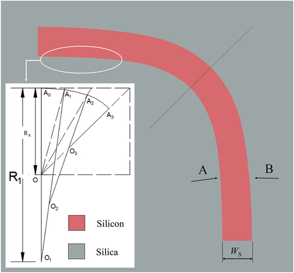
Fig. 1. Proposed MWB based on the DFFC design. DFFC consists of curve A and curve B, and WS is the width of the MWB. The inset shows a schematic diagram of the change of curvature radius, and RA is the equivalent radius of the free-form curve A.
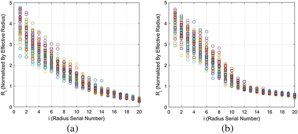
Fig. 2. Proper combinations of (a) curve A and (b) curve B are given. Here the ordinate represents a multiple of the equivalent radius.
Fig. 3. Simulation results of the DFFC–MWB with an input width WS=1.1 μm. (a)–(c) Simulated optical field distributions in the designed MWB based on the DFFC with TE0, TE1, and TE2 modes, respectively. (d)–(f) Calculated transmission spectra for three modes in the wavelength range of 1.5–1.6 μm. Herein the dotted line corresponds to the axis on the left, and the real line corresponds to the axis on the right.
Fig. 4. Simulation results of the DFFC–MWB with an input width WS=1.48 μm and an equivalent radius of 10 μm. (a)–(d) Simulated optical field distributions in the device with four mode channels at 1.55 μm. (e)–(h) Calculated transmission spectra of the four-mode bent waveguide in the wavelength range of 1.5–1.6 μm. Herein the dotted line corresponds to the axis on the left, and the real line corresponds to the axis on the right.
Fig. 5. Transmittance spectra of the MWB based on the DFFC with ΔW varying from −80 to 80 nm. (a)–(d) Transmission efficiencies of the four modes at 1550 nm. Simulation results show that this device has large fabrication tolerance.
Fig. 6. Microscopic view of the fabricated silicon multimode bends with four mode channels. The multiplexer and demultiplexer are connected with (a) straight multimode waveguide or (b) eight cascaded 90° MWBs based on the DFFC. (c) SEM image of the cascaded MWBs.
Fig. 7. Measured spectra of the normalized transmittances of a single four-mode waveguide bend. (a)–(h) Measurement results of a single 90° four-mode bend based on (a)–(d) DFFC or (e)–(h) SFFC.
Mode | (μm) | Method | | | | | | | | |
---|
Three | 1.1 | DFFC | 0.0084 | −31.38 | 0.0128 | −31.34 | 0.1746 | −39.33 | / | / | SFFC | 0.0080 | −32.07 | 0.0168 | −26.74 | 0.3398 | −26.63 | / | / | Four | 1.48 | DFFC | 0.0191 | −29.61 | 0.0219 | −29.92 | 0.0231 | −29.47 | 0.1291 | −29.82 | SFFC | 0.0415 | −23.09 | 0.0386 | −23.08 | 0.0318 | −27.35 | 0.0619 | −31.59 |
|
Table 1. Calculated Results Related to Different Device Parameters for Comparisona
Reference | Method | | (μm) | EL (dB) | CT (dB) |
---|
Theory | Meas. | Theory | Meas. |
---|
[21] | SWG tapers | 4 | 45.8 | 0.4 | 1 | −20 | −20 | [22] | SWGs | 3 | 10 | 0.5 | 0.7 | −30 | −20 | 4 | 20 | 0.5 | 0.8 | −26 | −15 | [23] | Euler curves | 4 | 45 | 0.1 | 0.5 | −25 | −20 | [24] | Bezier curves | 3 | 20 | 0.2 | / | −26 | −23 | [25] | Corner bend | 2 | 7 | 0.18 | 0.53 | −36 | −15 | 10 | 35 | 0.54 | / | −24 | / | [26] | TO-optimized | 4 | 17 | 0.1 | 0.55 | −20 | −17 | [27] | SFFC | 3 | 9.35 | 0.04 | 0.2 | −29 | −25 | This work | DFFC | 3 | 6 | 0.17 | / | −31 | / | 4 | 10 | 0.13 | 0.72 | −29 | −25 |
|
Table 2. Comparison of the Reported Results of Silicon Multimode Waveguide Bendsa