
Ding SUN, Yanyan DING, Lingwei KONG, Yuhong ZHANG, Xiujuan GUO, Liming WEI, Li ZHANG, Lixin ZHANG. First-principles Study on Mg Doping in Cu2ZnSnS4 [J]. Journal of Inorganic Materials, 2020, 35(11): 1290
- Journal of Inorganic Materials
- Vol. 35, Issue 11, 1290 (2020)
Abstract
The kesterite Cu2ZnSn(S,Se)4 (CZTSSe) based compound solar cells has attracted a great number of attentions because of the non-toxicity and abundance of the constituent elements[
Recently, Mg-doped CZTS(Se) materials have been synthesized by many techniques such as ultrasonic co-spray method[
1 Computational details
In the present work, all calculations have been performed based on density functional theory (DFT) as implanted in the VASP code[
Screened Coulomb hybrid functional Heyd-Scuseria- Ernzerhof (HSE06)[
Mg-related point defects including three antisites MgCu, MgZn and MgSn are considered (one Mg atom substitutes Cu, Zn and Sn site, respectively). The defect formation energies are calculated as[
where Eα,q and Eh is the total energy of the supercell with and without a defect α, respectively. Ei is the total energy of the component element i in its pure phase; ni is the number of atoms i removed from the supercell in forming the defect with the chemical potential μi in forming the defect α. The μi is referenced to the total energy Ei of the elemental solid and μi=0 means the element is so rich that the pure element phase can form. EF is the Fermi energy, which varies from valence band maximum (VBM) of the host, denoted by εVBM, to the conduction band minimum (CBM) for non-degenerate semiconductors. Because of the finite size of supercells, the Lany and Zunger correction method[
2 Results and discussion
The predicted lattice parameters and bandgap results by using two types of exchange-correlation functionals are presented in Table 1. HSE06 functional predicts a bandgap of 1.45 eV for CZTS, in consistent with the experimental values. By contrast, the PBE functional largely underestimate the bandgap. Therefore, HSE06 is used to calculate the electronic structures and defect properties of Mg-doped CZTS.
![]()
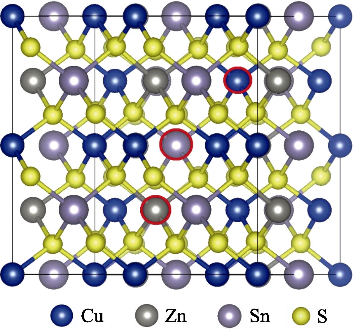
Figure 1.Supercell used to calculate the defect properties of Mg-doped CZTS, where the red circles denote the locations of the antisite defects
A defect often produces states within the band gap, with the stronger the gap states, the more localization of the defect charge distribution. The charge localization feature can be seen from the band structures, as shown in Fig. 2. The charge states of MgCu and MgSn are similar to ZnCu and ZnSn which are both charge delocalized defects[
| Functional | Band gap/eV | ||
|---|---|---|---|
| PBE | 0.5471 | 1.0944 | 0.51 |
| HSE | 0.5469 | 1.0935 | 1.45 |
| Expt.[ | 0.5427 | 1.0871 | 1.44-1.51 |
Table 1.
Lattice parameters a and c and band gaps of CZTS as obtained using PBE and HSE compared to experimental values
Whether a defect level could significantly affect the solar cell performance also depends on its concentration which is related to the formation energy, a function of the elemental chemical potentials and Fermi level according to eq. (1). And the stable region of chemical potential is needed to be determined before performing the calculation of formation energies of the Mg-related defects. A series of thermodynamic conditions must be satisfied by the chemical potentials:
(I) The sum of the chemical potentials of the component elements should maintain a stable host compound, which means:
where ΔHf (Cu2ZnSnS4) relates to the formation energy of Cu2ZnSnS4.
(II) The formation of pure elemental phase should be avoided. Thus, the atomic chemical potentials in CZTS should be smaller than that of the corresponding elemental solid. That is:
(III) The formation of all other secondary compounds including CuS, Cu2S, ZnS, SnS, SnS2, Cu2SnSe3 and MgS should be avoided, as described by the following relations:
${{\mu }_{\text{Cu}}}\text{+}{{\mu }_{\text{S}}}\text{}\Delta {{H}_{\text{f}}}(\text{CuS})=-0.\text{53 eV}$
$2{{\mu }_{\text{Cu}}}\text{+}{{\mu }_{\text{S}}}\text{}\Delta {{H}_{\text{f}}}(\text{C}{{\text{u}}_{\text{2}}}\text{S})=-0.94\text{ eV}$
${{\mu }_{\text{Zn}}}\text{+}{{\mu }_{\text{S}}}\text{}\Delta {{H}_{\text{f}}}(\text{ZnS})=-1.96\text{eV}$
${{\mu }_{\text{Sn}}}\text{+}{{\mu }_{\text{S}}}\text{}\Delta {{H}_{\text{f}}}(\text{SnS})=-0.84\text{ eV}$
$2{{\mu }_{\text{Cu}}}\text{+}{{\mu }_{\text{Sn}}}\text{+}3{{\mu }_{\text{S}}}\text{}\Delta {{H}_{\text{f}}}(\text{C}{{\text{u}}_{\text{2}}}\text{Sn}{{\text{S}}_{3}})=-2.64\text{ eV}$
${{\mu }_{\text{Mg}}}\text{+}{{\mu }_{\text{S}}}\text{}\Delta {{H}_{\text{f}}}(\text{MgS})=-3.14\text{ eV}$
With the thermodynamic conditions established, the stable chemical potential region of CZTS is confined in a three-dimensional space. As a result of Equation 2, there can be only three independent variables for CZTS, such as μCu, μZn and μSn. Here we take the chemical potential range determined by Zhang et al.[
![]()
Figure 2.Band structures of the host CZTS and the MgCu, MgZn and MgSn with different charge states
![]()
Figure 3.Stable chemical potential region of CZTS(considering the Mg induced secondary phase MgS) with
To figure out the microscopic mechanism of Mg-doping, the formation energies as a function of EF for Mg-related defects at points A-D are calculated. Whereas we only show the results at point D since Zn-rich growth condition is preferred by CZTS solar cells with high efficiency. As shown in Fig. 4, the formation energies of MgCu+ and MgZn0 are lower than 2 eV in the whole EF range, which means these defects can exist in large amount in CZTS. By contrast, the formation energy of MgSn2- is higher than 2 eV when EF is closed to the VBM.
| Point | D | D | D | D |
|---|---|---|---|---|
| A | -0.5 | -1.93 | -1.76 | -3.11 |
| B | -0.5 | -2.14 | -1.55 | -3.11 |
| C | -0.5 | -1.97 | -1.04 | -2.94 |
| D | -0.5 | -1.76 | -1.25 | -2.94 |
Table 2.
Chemical potentials at the A-D points labeled in
![]()
Figure 4.The formation energies of Mg-related defects as a function of Fermi energy at point D shown in
It is also found that the formation energy of MgZn0 is even smaller than that of MgCu+ in large EF range, which indicates that the Mg atom prefers to substitute the Zn atomic site in CZTS. Since Mg and Zn are isovalent, the MgZn will not affect the conduction type. Moreover, the existence of MgZn makes it easy for other Cu atoms to be substituted by Mg atom. The comparison of the formation energy of MgCu in the supercell with and without a Mg dopant on the Zn site is shown in Fig. 5. With Mg dopant, the formation energy of MgCu+ decreases by 52 meV than that without Mg atom. The Bader charge shows that the amount of transferred electron from Mg to S is larger than that of Zn in CZTS, as shown in Fig. 6. Thus, it compensates electrons transferred from other Cu atoms to obey the Octet rule which makes the Coulomb attraction between Cu-S weaker than that in pure CZTS. As a result, it is easier for Cu atom to be substituted by Mg atom, and Mg doping promotes the population of MgCu donor.
![]()
Figure 5.The comparison of the formation energy of MgCu in pure CZTS and Mg doped CZTS as a function of chemical potential at points A, B, C and D shown in
A buried p-n junction in Cu(InGa)Se2 (CIGS) film facilitates electron-hole separation of photogenerated carriers. Some groups attempted doping of Cd into CIGS films to convert the near-interface region from p-type CIGS to n-type to improve the performances[
![]()
Figure 6.The difference density charge (including Bader charges) for Mg doped CZTS
3 Conclusions
In this work, we have carried out hybrid functional computations on the Mg-related defect properties in CZTS. According to our results, all Mg-related defects are not charge localized defects and will not produce deep defect levels within the bandgap. Furthermore, MgCu and MgZn have very low formation energies in large EF range. Besides the well-established Cu-poor and Zn-rich growth conditions, Sn-rich growth condition is proposed to suppress MgSn. Under these conditions, Mg prefers to occupy the Cu atomic site and acts as shallow donor. Finally, we suggest that Mg doping on the surface might be an effective method to further improve the efficiency of Cu2ZnSnS4-based solar cells.
References
[1] B MITZI D, O GUNAWAN, K TODOROV T et al. The path towards a high-performance solution-processed kesterite solar cell. Sol. Energy Mater. Sol. Cells, 95, 1421-1436(2011).
[2] W WANG, T WINKLER M, O GUNAWAN et al. Device characteristics of CZTSSe thin-film solar cells with 12.6% efficiency. Adv. Energy Mater., 4, 1301465(2013).
[3] W SHOCKLEY, H QUEISSER. Detailed balance limit of efficiency of p-n junction solar cells. J. Appl. Phys., 32, 510-519(1961).
[4] T GOKMEN, O GUNAWAN, K TODOROV T et al. Band tailing and efficiency limitation in kesterite solar cells. Appl. Phys. Lett., 103, 103506(2013).
[5] L MENG, F LI Y, B YAO et al. Mechanism of effect of intrinsic defects on electrical and optical properties of Cu2CdSnS4: an experimental and first-principles study. J. Phys. D Appl. Phys., 48, 445105(2015).
[6] F OZEL, M KUS, A YAR et al. Fabrication of quaternary Cu2FeSnS4(CFTS) nanocrystalline fibers through electrospinning technique. J. Mater. Sci., 50, 777-783(2015).
[7] J YU J, M DENG H, Q ZHANG et al. The role of sulfurization temperature on the morphological, structural and optical properties of electroplated Cu2MnSnS4 absorbers for photovoltaics. Mater. Lett., 233, 111-114(2018).
[8] I SAPELI M M, T FERDAOUS M, A SHAHAHMADI S et al. Effects of Cr doping in the structural and optoelectronic properties of Cu2ZnSnS4(CZTS) thin film by magnetron co-sputtering. Mater. Lett., 221, 22-25(2018).
[9] K MATSUBARA, A YAMADA, S ISHIZUKA et al. Wide-gap CIGS solar cells with Zn1-
[13] T MAEDA, S NAKAMURA, T WADA. First-principles study on Cd doping in Cu2ZnSnS4 and Cu2ZnSnSe4. Jpn. J. Appl. Phys, 51(2012).
[14] D SUN, Y DING Y, W KONG L et al. First principles calculation of the electronic-optical properties of Cu2MgSn(S
[15] Y XIAO Z, Y LI, B YAO et al. Bandgap engineering of Cu2Cd
[16] G KRESSE, J FURTHMUELLER. Efficiency of
[17] G KRESSE, D JOUBERT. From ultrasoft pseudopotentials to the projector augmented-wave method. Phys. Rev. B, 59, 1758-1775(1999).
[18] J HEYD, E SCUSERIA G, M ERNZERHOF. Hybrid functionals based on a screened Coulomb potential. J. Chem. Phys., 118, 8207-8215(2003).
[20] W XIAO, N WANG J, S ZHAO X et al. Intrinsic defects and Na doping in Cu2ZnSnS4: a density-functional theory study. Sol. Energy, 116, 125-132(2015).
[22] S LANY, A ZUNGER. Assessment of correction methods for the band-gap problem and for finite-size effects in supercell defect calculations: case studies for ZnO and GaAs. Phys. Rev. B, 78, 1879-1882(2008).
[23] U DASGUPTA, K SAHA S, J PAL A. Fully-depleted pn-junction solar cells based on layers of Cu2ZnSnS4 (CZTS) and copper-diffused AgInS2 ternary nanocrystals. Sol. Energy Mater. Sol. Cells, 124, 79-85(2014).
[24] P KOMSA H, T RANTALA T, A PASQUARELLO. Finite-size supercell correction schemes for charged defect calculations. Phys. Rev. B., 86, 045112(2012).
[25] J PAIER, R ASAHI, A NAGOYA et al. Cu2ZnSnS4 as a potential photovoltaic material: a hybrid Hartree-Fock density functional theory study. Phys. Rev. B, 79, 115126.
[26] L ZHANG X, M HAN M, H ZHENG X et al. The suppression of Cu-related charge localized defects in Cu2ZnSnS4 thin film solar cells. Sol. Energy Mater. Sol. Cells, 180, 118-122(2018).
[27] L ZHANG X, M HAN M, Z ZHENG et al. The instability of S vacancies in Cu2ZnSnS4. RSC Adv, 6, 15424-15429(2016).
[28] L ZHANG X, M HAN M, Z ZHENG et al. The role of Sb in solar cell material Cu2ZnSnS4. J. Mater. Chem. A, 5, 6606-6612(2017).
[29] N NAGHAVI, D ABOU-RAS, N ALLSOP et al. Buffer layers and transparent conducting oxides for chalcopyrite Cu(In,Ga)(S,Se)2 based thin film photovoltaics: present status and current developments. Prog. Photovoltaics, 18, 411-433(2010).


Set citation alerts for the article
Please enter your email address

© Copyright 2018-2021 | Chinese Laser Press. All Rights Reserved 沪ICP备15018463号-20