• Journal of Semiconductors
  • Vol. 43, Issue 9, 092801 (2022)
Yabao Zhang1、2, Jun Zheng1、2、*, Peipei Ma1、2, Xueyi Zheng1、3, Zhi Liu1、2, Yuhua Zuo1、2, Chuanbo Li3, and Buwen Cheng1、2
Author Affiliations
  • 1State Key Laboratory on Integrated Optoelectronics, Institute of Semiconductors, Chinese Academy of Sciences, Beijing 100083, China
  • 2Center of Materials Science and Optoelectronics Engineering, University of Chinese Academy of Sciences, Beijing 100049, China
  • 3School of Science, Minzu University of China, Beijing 100081, China
  • show less
    DOI: 10.1088/1674-4926/43/9/092801 Cite this Article
    Yabao Zhang, Jun Zheng, Peipei Ma, Xueyi Zheng, Zhi Liu, Yuhua Zuo, Chuanbo Li, Buwen Cheng. Growth and characterization ofβ-Ga2O3 thin films grown on off-angled Al2O3 substrates by metal-organic chemical vapor deposition[J]. Journal of Semiconductors, 2022, 43(9): 092801 Copy Citation Text show less
    (Color online) XRD patterns ofβ-Ga2O3 films deposited onc-plane Al2O3 substrates with different off-axis angles toward 112¯0>.
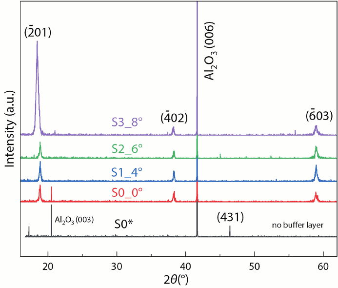
    Fig. 1. (Color online) XRD patterns ofβ-Ga2O3 films deposited onc-plane Al2O3 substrates with different off-axis angles toward < 112¯0>.
    (Color online) (a) XRD rocking curves of the (2¯01) diffraction peaks ofβ-Ga2O3 films deposited onc-plane Al2O3 substrates with different off-axis angles toward 112¯0>, (b) FWHM as a function of off-axis angles of Al2O3 substrates.
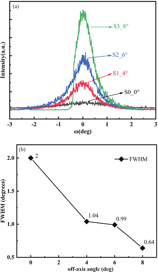
    Fig. 2. (Color online) (a) XRD rocking curves of the ( 2¯01) diffraction peaks ofβ-Ga2O3 films deposited onc-plane Al2O3 substrates with different off-axis angles toward < 112¯0>, (b) FWHM as a function of off-axis angles of Al2O3 substrates.
    Cross-sectional TEM of the film deposited on an 8° off-axis sapphire substrate with a thickness of 300 nm. (a) Image of the whole film. (b) HRTEM micrograph of the interface. (c) Selected area electron diffraction (SAED) obtained by Fourier transform of area B. (d) Selected area electron diffraction (SAED) obtained by Fourier transform of area A.
    Fig. 3. Cross-sectional TEM of the film deposited on an 8° off-axis sapphire substrate with a thickness of 300 nm. (a) Image of the whole film. (b) HRTEM micrograph of the interface. (c) Selected area electron diffraction (SAED) obtained by Fourier transform of area B. (d) Selected area electron diffraction (SAED) obtained by Fourier transform of area A.
    (Color online) 10 × 10μm2 AFM patterns ofβ-Ga2O3 films deposited on (a) 0°, (b) 4°, (c) 6° and (d) 8° off-axis Al2O3 substrates. All films were annealed in-situ for 10 min under an oxygen atmosphere.
    Fig. 4. (Color online) 10 × 10μm2 AFM patterns ofβ-Ga2O3 films deposited on (a) 0°, (b) 4°, (c) 6° and (d) 8° off-axis Al2O3 substrates. All films were annealed in-situ for 10 min under an oxygen atmosphere.
    SEM ofβ-Ga2O3 thin films on Al2O3 substrates with (a) 0°, (b) 4°, (c) 6°, and (d) 8° off-angles toward 112¯0>.
    Fig. 5. SEM ofβ-Ga2O3 thin films on Al2O3 substrates with (a) 0°, (b) 4°, (c) 6°, and (d) 8° off-angles toward < 112¯0>.
    (Color online) (a) Room temperature PL spectra of all films grown on off-angled Al2O3 substrates. The broad emission band from ultraviolet to blue of theβ-Ga2O3 film deposited on (b) 4°, (c) 6°, and (d) 8° can be divided into two emission peaks near 365 and 410 nm.
    Fig. 6. (Color online) (a) Room temperature PL spectra of all films grown on off-angled Al2O3 substrates. The broad emission band from ultraviolet to blue of theβ-Ga2O3 film deposited on (b) 4°, (c) 6°, and (d) 8° can be divided into two emission peaks near 365 and 410 nm.
    Yabao Zhang, Jun Zheng, Peipei Ma, Xueyi Zheng, Zhi Liu, Yuhua Zuo, Chuanbo Li, Buwen Cheng. Growth and characterization ofβ-Ga2O3 thin films grown on off-angled Al2O3 substrates by metal-organic chemical vapor deposition[J]. Journal of Semiconductors, 2022, 43(9): 092801
    Download Citation