Abstract
Beta-gallium oxide (β-Ga2O3) thin films were deposited onc-plane (0001) sapphire substrates with different mis-cut angles along < > by metal-organic chemical vapor deposition (MOCVD). The structural properties and surface morphology of as-grownβ-Ga2O3 thin films were investigated in detail. It was found that by using thin buffer layer and mis-cut substrate technology, the full width at half maximum (FWHM) of the ( ) diffraction peak of theβ-Ga2O3 film is decreased from 2° onc-plane (0001) Al2O3 substrate to 0.64° on an 8° off-angledc-plane (0001) Al2O3 substrate. The surface root-mean-square (RMS) roughness can also be improved greatly and the value is 1.27 nm for 8° off-angledc-plane (0001) Al2O3 substrate. Room temperature photoluminescence (PL) was observed, which was attributed to the self-trapped excitons formed by oxygen and gallium vacancies in the film. The ultraviolet–blue PL intensity related with oxygen and gallium vacancies is decreased with the increasing mis-cut angle, which is in agreement with the improved crystal quality measured by high resolution X-ray diffraction (HR-XRD). The present results provide a route for growing high qualityβ-Ga2O3 film on Al2O3 substrate.Beta-gallium oxide (β-Ga2O3) thin films were deposited onc-plane (0001) sapphire substrates with different mis-cut angles along < > by metal-organic chemical vapor deposition (MOCVD). The structural properties and surface morphology of as-grownβ-Ga2O3 thin films were investigated in detail. It was found that by using thin buffer layer and mis-cut substrate technology, the full width at half maximum (FWHM) of the ( ) diffraction peak of theβ-Ga2O3 film is decreased from 2° onc-plane (0001) Al2O3 substrate to 0.64° on an 8° off-angledc-plane (0001) Al2O3 substrate. The surface root-mean-square (RMS) roughness can also be improved greatly and the value is 1.27 nm for 8° off-angledc-plane (0001) Al2O3 substrate. Room temperature photoluminescence (PL) was observed, which was attributed to the self-trapped excitons formed by oxygen and gallium vacancies in the film. The ultraviolet–blue PL intensity related with oxygen and gallium vacancies is decreased with the increasing mis-cut angle, which is in agreement with the improved crystal quality measured by high resolution X-ray diffraction (HR-XRD). The present results provide a route for growing high qualityβ-Ga2O3 film on Al2O3 substrate.Introduction
In recent years, Ga2O3 has gained considerable attention in transparent electrodes, solar-blind ultraviolet detectors, flame sensors and power devices[1-4] thanks to its ultrawide bandgap (4.5–4.9 eV)[5] and high critical breakdown field (8 MV/cm)[6]. Monoclinic crystalβ-Ga2O3 has the highest thermal stability among the five phases of gallium oxide[7], and its Baliga's figure of merit (BFOM) is 3.8 and 10.14 times that of the third-generation semiconductors GaN and 4H-SiC, respectively[8]. Although homogeneous substrates are the ideal choice for growingβ-Ga2O3 films, the preparation process for large size gallium oxide wafer is immature and its cost is still expensive when compared with Al2O3 substrates. Moreover, the thermal conductivity of gallium oxide is relatively poor, with values of 15.4%, 4.7% and 1.2% for silicon, 4H-SiC and diamond, respectively. Hence, theβ-Ga2O3 obtained by heteroepitaxy is important for devices that generate amount of heat during operation.
There are several reports about the growth of high-quality Ga2O3 on foreign substrates[9]. Maet al. tried to grow Ga2O3 on substrates such as SrTiO3(100)[10], epi-GaN/sapphire (0001)[11], MgO(111)[12] and MgAl6O10[13] by using MOCVD. However, these thin films were obtained by heteroepitaxy and have multiple crystal domains, which will affect the transport properties of carriers[14]. Among the different substrates, sapphire substrates are widely studied due to their low cost and smaller lattice mismatch with Ga2O3. Substantial effort has been devoted to grow high-quality Ga2O3 single crystals on sapphire substrates[15-20]. However,β-Ga2O3 and sapphire belong to different crystal phases, and multiple crystal domains will appear because of random nucleation during growth. Using sapphire substrates with off-axis angle, it was shown that the crystallinity of epitaxialβ-Ga2O3 films can be improved by controlling the crystal domains. Oshimaet al. have grown Ga2O3 on off-axis substrates by HVPE and found that the (310) oriented domains disappeared when off-axis angles beyond 3°[21]. It was also found that the off-angled sapphire substrates can change the growth mode ofβ-Ga2O3 films from six-fold in-plane rotational domain growth to single quadrilateral-domains growth[22].
In this paper, we reportβ-Ga2O3 epitaxial layers on Al2O3 substrates with different off-axis angles. The structural properties ofβ-Ga2O3 were studied, and it was found that the surface topography ofβ-Ga2O3 films can be greatly improved by using a buffer layer and off-angled sapphire substrates. The ultraviolet to blue light emission related with oxygen and gallium vacancies was observed and the PL mechanism was investigated.
Experimental
Film growth
Crystalβ-Ga2O3 thin films were grown onc-plane Al2O3 substrates (Two-inch, single polished) with different off-angles (0°, 4°, 6° and 8°, corresponding to sample Nos. S0-S3) by using MOCVD (Aixtron Ltd) under the same conditions. For comparison, a Ga2O3 film (No. S0*) was also deposited without a buffer layer. Trimethylgallium (TMGa, 6N), which was stored in a stainless-steel bubbler maintained at 5 °C, and O2 (purity, 5N) were used as precursors for gallium and oxygen, respectively. High-purity argon (Ar, 5N) was applied as the carrier gas to deliver TMGa vapor to the reactor chamber by passing through the TMGa bubbler. Prior to growingβ-Ga2O3 thin films at 960 °C with an O2/TMGa source flow about 2000 sccm/30 sccm (standard cubic centimeter per minute), a 10 nm thick Ga2O3 buffer layer was deposited at 800 °C with an O2/TMGa source flow about 1000 sccm/5 sccm. During the growth process, an excess oxygen source was used to avoid the formation of a large number of oxygen vacancies in the crystal. Finally, the metal organic source and oxygen cracking efficiency reached 9.5% and 0.7‰, respectively. The chamber pressure was maintained at 100 mbar during the entire growth process.
Characterization method
The as-grown film thickness was approximately 300 nm with the growth rate about 0.7μm/h. Atomic force microscopy (AFM) and scanning electron microscopy (SEM) were used to characterize the surface morphology of the samples. HR-XRD and high-resolution transmission electron microscopy (HR-TEM) were carried out to characterize the crystal phase and quality. The room temperature photoluminescence (PL) was measured by using a 213 nm laser as excited source. The PL signal was guided into a monochromator and detected by photomultiplier.
Results and discussion
Effects of off-axis angles of Al2O3 substrates on crystal quality
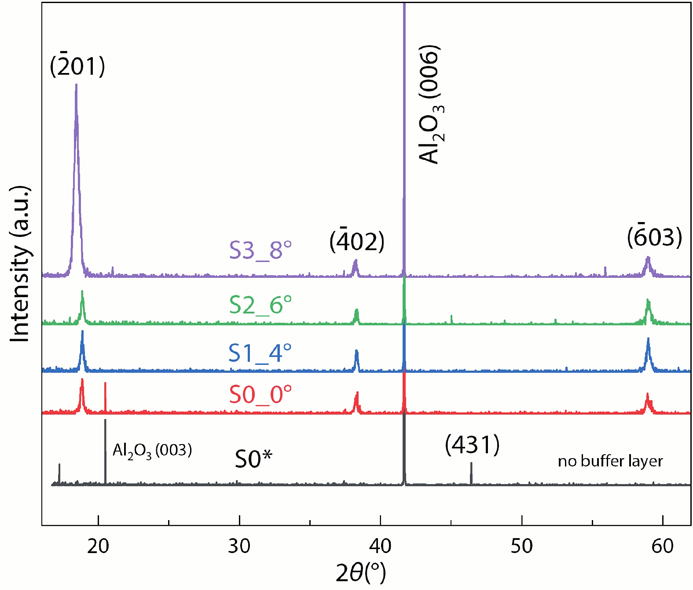
The crystal quality of the gallium oxide thin films grown on sapphire substrates was characterized by HR-XRD in theω–2θ configuration, as shown inFig. 1. For the film grown on sapphire substrate (S0*) without a buffer layer, the XRD spectrum shows totally different pattern. By comparing to PDF #06-0529, the appearance of a diffraction peak centered at 46.43° may belong to the δ-Ga2O3 domains. Zhuoet al. reported that when Ga2O3 was first deposited on Al2O3 substrates, there were nuclei of various phases[17]. This result also proves that the existence of the buffer layer promoted the growth ofβ-Ga2O3. However, for the films grown on Al2O3 substrates with a buffer layer, three sharp diffraction peaks located at 18.45°, 38.29° and 58.95° are observed, which belong to the (
), (
) and (
) planes ofβ-Ga2O3 (compared to JCPDS No. 43-1012). These results show that the obtained gallium oxide films with a buffer layer are pureβ-Ga2O3 without any other gallium oxide phase. The preferential crystal growth direction is (
) because the arrangement of oxygen atoms in theβ-Ga2O3 (
) plane is equivalent to sapphire (0001)[15].Fig. 2 shows the XRD rocking curves at the (
) diffraction peak of the four samples. With the increasing substrates off-axis angles, the XRD peak intensity increases and the full width at half maximum (FWHM) of the (
) diffraction peak is decreased, reaching 0.64° for the film deposited on an 8° off-angled substrate. To illustrate the effect of the buffer layer clearly,β-Ga2O3 film without a buffer layer was also grown on the Al2O3 substrate with 8° off-axis angles toward \lt
\gt . Very weak X-ray diffraction peak belong to (
), (
) and (
) was observed and the RMS value was 7.5 nm (the RMS value for the film with a buffer is 1.27 nm), from the AFM measurement. (Figures not shown here.) This indicates that the surface topography ofβ-Ga2O3 films grown on off-angled Al2O3 substrates can be improved by introducing a buffer layer prior to thick film growth.

Figure 1.(Color online) XRD patterns ofβ-Ga2O3 films deposited onc-plane Al2O3 substrates with different off-axis angles toward <
>.
Figure 2.(Color online) (a) XRD rocking curves of the (
) diffraction peaks ofβ-Ga2O3 films deposited onc-plane Al2O3 substrates with different off-axis angles toward <
>, (b) FWHM as a function of off-axis angles of Al2O3 substrates.
To explain the role of buffer layer and mis-cut substrate angle, HR-TEM experiments were carried out. As shown inFig. 3(a), the step is clearly visible along the <
\gt direction of the Al2O3 substrate. The (
) plane distance of the epitaxial layer is calculated to be 0.466 nm by performing a Fourier transform on the region selected by the yellow dashed box inFig. 3(b). As the thickness of the epitaxial layer increases, the atoms are arranged more orderly and most dislocations are successfully constrained in the thin buffer layer.Figs. 3(c) and3(d) show the SAED patterns of buffer layer near and away the Ga2O3 films/Al2O3 interface, respectively. The SAED pattern consists of multiple sets of diffraction spots near the interface and became more regular in region A. This indicates that there were other phases of Ga2O3 in the initial growth period and the epitaxial layer gradually became pureβ-Ga2O3 as the film continued to grow. Thus, the great improvement in crystal quality is likely to happen because mis-cut sapphire can inhibit the appearance of the crystal domain by the strong in-plane orientation enhancement[23] and the buffer layer can accommodate most defects.
Figure 3.Cross-sectional TEM of the film deposited on an 8° off-axis sapphire substrate with a thickness of 300 nm. (a) Image of the whole film. (b) HRTEM micrograph of the interface. (c) Selected area electron diffraction (SAED) obtained by Fourier transform of area B. (d) Selected area electron diffraction (SAED) obtained by Fourier transform of area A.
Effects of off-axis angles of Al2O3 substrates onβ-Ga2O3film surface morphology
Fig. 4 shows the AFM image ofβ-Ga2O3 films deposited on different off-axis Al2O3 substrates. The measured surface RMS roughness values of samples S0, S1, S2 and S3 are 6, 2.58, 3.55 and 1.27 nm, respectively. The film deposited on an 8° off-axis Al2O3 substrate has the lowest RMS roughness. The RMS value in this work is much lower than the reported values grown on off-angled Al2O3 substrates[24]. There are many tiny domains on the surface of the as-grown sample, indicating that the growth changes from a two-dimensional plane growth to a three-dimensional island-like growth pattern. To further reveal the low RMS values of those grown on off-axis sapphire substrates, the surface morphology ofβ-Ga2O3 films was also characterized by SEM, as demonstrated inFig. 5. The surface domain of the films deposited on mis-cut sapphire substrates seems more closely due to step-flow growth[25] and the film surface shows a corrugated shape, which is the phenomenon of step bunching[26].
Figure 4.(Color online) 10 × 10μm2 AFM patterns ofβ-Ga2O3 films deposited on (a) 0°, (b) 4°, (c) 6° and (d) 8° off-axis Al2O3 substrates. All films were annealed in-situ for 10 min under an oxygen atmosphere.
Figure 5.SEM ofβ-Ga2O3 thin films on Al2O3 substrates with (a) 0°, (b) 4°, (c) 6°, and (d) 8° off-angles toward <
>.
PL properties ofβ-Ga2O3 films on off-angled Al2O3 substrates
PL spectrum is an effective method to investigate the defects of as-grownβ-Ga2O3 thin films.Fig. 6 shows the room temperature (297 K) PL spectra ofβ-Ga2O3 thin films excited by a 213 nm laser. Compared with the samples grown on the off-axis substrates (S1, S2 and S3), the luminescence of the sample S0 grown on the normal Al2O3 substrate is significantly weaker, which is due to the large number of non-radiative recombination centers generated by the crystal domain interface. The PL spectra have a broad emission band from ultraviolet to blue. The broad emission can be divided into two emission peaks near 365 and 410 nm, as shown inFigs. 6(b)–6(d). Varleyet al. reported that self-trapped holes (STHs) were widespread inβ-Ga2O3 and localized mainly on a single O atom in the lattice with the shape characteristic of an O 2p orbital[27]. The 365 nm peak is the process of radiative recombination between STHs and electrons to form STEs. This process has a strong electron-phonon coupling effect and local lattice distortion can cause the spectral broadening. The blue emission is overlapped at the UV band tail, which has been widely reported and is suggested to be related to donor-acceptor-pair recombination between VO donor and VGa or VGa–VO complex acceptors[27,28]. The radiative recombination luminescence from the conduction band and valence band ofβ-Ga2O3 is not observed in all samples, which is likely to be due to the fast non-radiative transition to the self-trapped energy level. As shown inFig. 6(a), the PL intensity is the strongest for the S1 sample and decreases with increasing substrate off-axis angles. Thus, the decrease in PL intensity indicates that the density of O and Ga vacancies are reduced. This is in accordance with the improved crystal quality from the XRD measurement.
Figure 6.(Color online) (a) Room temperature PL spectra of all films grown on off-angled Al2O3 substrates. The broad emission band from ultraviolet to blue of theβ-Ga2O3 film deposited on (b) 4°, (c) 6°, and (d) 8° can be divided into two emission peaks near 365 and 410 nm.
Conclusion
In summary,β-Ga2O3 thin films were successfully grown onc-plane mis-cut Al2O3 substrates. Our results showed that the quality of theβ-Ga2O3 thin films was improved by step-flow growth, and the FWHM of the (
) plane of the film deposited on an 8° off-angled substrate was 0.64°. It was revealed that the dislocations were mainly blocked by the buffer as observed by TEM measurement. The surface RMS roughness can also be reduced for theβ-Ga2O3 films deposited on off-axis Al2O3 substrates, reaching about 1.27 nm. Theβ-Ga2O3 film had broad light emission from ultraviolet to blue, which was attributed to the oxygen vacancies and gallium vacancies in the films. This vacancy related PL intensity was decreased with increasing off-angle, showing the improved crystalline quality, which was consistent with the HR-XRD results. These findings are helpful for the fabrication of high performanceβ-Ga2O3 devices based on Al2O3 substrate in near future.
Acknowledgements
This work was supported in part by the National Key Research and Development Program of China (Grant No. 2018YFB2200500), the National Natural Science Foundation (Grant Nos. 62050073, 62090054, 61975196).
References
[1] Y J Jeong, J Y Yang, C H Lee et al. Fluorine-based plasma treatment for hetero-epitaxialβ-Ga2O3 MOSFETs. Appl Surf Sci, 558, 149936(2021).
[2] P R Jubu, F K Yam. Development and characterization of MSM UV photodetector based on gallium oxide nanostructures. Sens Actuator A, 312, 112141(2020).
[3] Y J Lv, X Y Zhou, S B Long et al. Enhancement-modeβ-Ga2O3 metal-oxide-semiconductor field-effect transistor with high breakdown voltage over 3000 V realized by oxygen annealing. Phys Status Solidi RRL, 14, 1900586(2020).
[4] H Dong, H W Xue, Q M He et al. Progress of power field effect transistor based on ultra-wide bandgap Ga2O3 semiconductor material. J Semicond, 40, 011802(2019).
[5] H H Tippins. Optical absorption and photoconductivity in the band edge ofβ-Ga2O3. Phys Rev, 140, A316(1965).
[6] N Ueda, H Hosono, R Waseda et al. Anisotropy of electrical and optical properties inβ-Ga2O3 single crystals. Appl Phys Lett, 71, 933(1997).
[7] J A Kohn, J D Broder. Characterization ofβ-Ga2O3 and its alumina isomorph,θ-Al2O3. Am Mineral, 42, 398(1957).
[8] S I Stepanov, V I Nikolaev, V E Bougrov et al. Gallium oxide: Properties and applications - A review. Rev Adv Mater Sci, 44, 63(2016).
[9] S J Pearton, J C Yang, P H Cary et al. A review of Ga2O3 materials, processing, and devices. Appl Phys Rev, 5, 011301(2018).
[10] D Wang, L N He, Y Le et al. Characterization of single crystalβ-Ga2O3 films grown on SrTiO3 (100) substrates by MOCVD. Ceram Int, 46, 4568(2020).
[11] Q Cao, L N He, H D Xiao et al. β-Ga2O3 epitaxial films deposited on epi-GaN/sapphire (0001) substrates by MOCVD. Mater Sci Semicond Process, 77, 58(2018).
[12] W Mi, J Ma, C N Luan et al. Characterization ofβ-Ga2O3 epitaxial films grown on MgO (111) substrates by metal-organic chemical vapor deposition. Mater Lett, 87, 109(2012).
[13] W Mi, C N Luan, Z Li et al. Ultraviolet-green photoluminescence ofβ-Ga2O3 films deposited on MgAl6O10 (100) substrate. Opt Mater, 35, 2624(2013).
[14] C Qian, J Sun, L Zhang et al. Crystal-domain orientation and boundary in highly ordered organic semiconductor thin film. J Phys Chem C, 119, 14965(2015).
[15] S Nakagomi, Y Kokubun. Crystal orientation ofβ-Ga2O3 thin films formed onc-plane and a-plane sapphire substrate. J Cryst Growth, 349, 12(2012).
[16] F Boschi, M Bosi, T Berzina et al. Hetero-epitaxy of ε-Ga2O3 layers by MOCVD and ALD. J Cryst Growth, 443, 25(2016).
[17] Y Zhuo, Z M Chen, W B Tu et al. β-Ga2O3 versus ε-Ga2O3: Control of the crystal phase composition of gallium oxide thin film prepared by metal-organic chemical vapor deposition. Appl Surf Sci, 420, 802(2017).
[18] D Q Hu, Y Wang, S W Zhuang et al. Surface morphology evolution and optoelectronic properties of heteroepitaxial Si-dopedβ-Ga2O3 thin films grown by metal-organic chemical vapor deposition. Ceram Int, 44, 3122(2018).
[19] J W Wu, W Mi, Z C Yang et al. Influence of annealing on the structural and optical properties of gallium oxide films deposited on c-sapphire substrate. Vacuum, 167, 6(2019).
[20] J Q Wei, K Kim, F Liu et al. β-Ga2O3 thin film grown on sapphire substrate by plasma-assisted molecular beam epitaxy. J Semicond, 40, 012802(2019).
[21] Y Oshima, E G Vίllora, K Shimamura. Quasi-heteroepitaxial growth ofβ-Ga2O3 on off-angled sapphire (0001) substrates by halide vapor phase epitaxy. J Cryst Growth, 410, 53(2015).
[22] W L Xu, J C Shi, Y W Li et al. Study ofβ-Ga2O3 films hetero-epitaxially grown on off-angled sapphire substrates by halide vapor phase epitaxy. Mater Lett, 289, 129411(2021).
[23] S Rafique, L Han, A T Neal et al. Towards high-mobility heteroepitaxialβ-Ga2O3 on sapphire–dependence on the substrate off-axis angle. Phys Status Solidi A, 215, 1700467(2018).
[24] T Zhang, Z G Hu, Y F Li et al. Investigation on theβ-Ga2O3 deposited on off-angled sapphire (0001) substrates. J Lumin, 233, 117928(2021).
[25] I Bryan, Z Bryan, S Mita et al. Surface kinetics in AlN growth: A universal model for the control of surface morphology in III-nitrides. J Cryst Growth, 438, 81(2016).
[26] M H Xie, S H Cheung, L X Zheng et al. Step bunching of vicinal GaN(0001) surfaces during molecular beam epitaxy. Phys Rev B, 61, 9983(2000).
[27] J B Varley, A Janotti, C Franchini et al. Role of self-trapping in luminescence andp-type conductivity of wide-band-gap oxides. Phys Rev B, 85, 081109(2012).
[28] C H Ho, C Y Tseng, L C Tien. Thermoreflectance characterization of beta-Ga2O3 thin-film nanostrips. Opt Express, 18, 16360(2010).