
Yuanjie Lü, Xubo Song, Zezhao He, Yuangang Wang, Xin Tan, Shixiong Liang, Cui Wei, Xingye Zhou, Zhihong Feng. Source-field-plated Ga2O3 MOSFET with a breakdown voltage of 550 V[J]. Journal of Semiconductors, 2019, 40(1): 012803
- Journal of Semiconductors
- Vol. 40, Issue 1, 012803 (2019)
Abstract
1. Introduction
Gallium oxide (Ga2O3) has recently attracted significant attention as a new semiconductor material for high-power and high-efficiency applications in recent years due to its outstanding characteristics such as ultra-wide bandgap (~4.8 eV), high critical electronic breakdown field (8 MV/cm), and low cost advantages[
Since the first β-Ga2O3 metal–semiconductor field-effect transistor (MESFET) was fabricated in 2012[
Our group reported a β-Ga2O3 MOSFET with HfO2 as a gate dielectric, in which the Ion/Ioff ratio was as high as 108. However, the three-terminal off-state breakdown voltage was just 113 V[
A field plate can suppress the peak electronic field in a MOSFET channel, and effectively improve the breakdown characteristics. In the reported Ga2O3 MOSFETs, a just gate-connected field plate was adopted, which increased the breakdown voltage greatly. A source-connected field plate is also a very effective option, which has been widely used in GaN and SiC based power devices. In this paper, a source-connected field plate was introduced into Ga2O3 MOSFETs for the first time resulting in increased high-breakdown voltage. The Ga2O3 MOSFETs were fabricated on homoepitaxial n-typed β-Ga2O3 film. High k HfO2 gate dielectric film formed by atomic layer deposition was adopted to reduce the gate leakage. In the device, gate-to-drain spacing (Lgd) of 4 μm was observed and three-terminal off-state breakdown voltage was measured as 450 V, and reached 550 V as the spacing increased to 8 μm. Finally, the breakdown voltage of 550 V is the highest among domestic reports.
2. Experiments
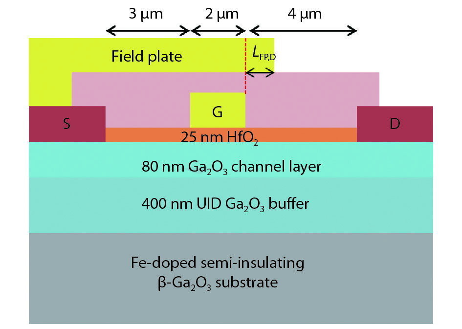
A schematic cross section of the fabricated Ga2O3 MOSFET is shown in Fig. 1. A 400 nm unintentionally doped (UID) Ga2O3 buffer layer and an 80 nm Si-doped channel layer were grown by metal organic chemical vapor deposition (MOCVD) on an Fe-doped semi-insulating (010) Ga2O3 substrate. The Si donor concentration was 1.0 × 1018 cm−3, whilst electron mobility was measured at 25 cm2/(V·s). Device fabrication began with mesa isolation, which was performed using BCl3/Ar inductively coupled plasma (ICP). The mesa height was about 200 nm. The source and drain Ohmic contacts were formed by depositing Ti/Au (15/200 nm) by using e-beam evaporation and lift-off technology. These contacts were annealed in a rapid thermal annealing system for 1 min at 480 °C in nitrogen. With a transmission line method pattern, the specific contact resistance was measured to be 8.5 Ω·mm. A 25 nm HfO2 gate dielectric layer was then deposited on the surface at 250 °C by atomic layer deposition. A Ni/Au Schottky contact was fabricated using e-beam evaporation and lift-off technology. As shown in Fig. 1, the gate length (Lg) and gate-to-source distance (Lgs) were set at 2 and 3 μm, respectively. The gate-to-drain spacing (Lgd) at 4, 8, 15, and 20 μm was also prepared. An 80 nm SiN passivation layer was deposited on the device surface by plasma enhanced chemical vapor deposition (PECVD). SiN/HfO2 recess was carried out on the source and drain regions by BCl3 reactive ion etching (RIE). Finally, a Ni/Au source-field plate was realigned to the source contact with a drain extension (LFP,D) of 0.8 μm (as shown in Fig. 1).
![]()
Figure 1.(Color online) Schematic cross section of the fabricated Ga2O3 MOSFET with
3. Results and discussion
Standard DC I–V measurements were performed using a semiconductor characterization system at room temperature. Fig. 2(a) illustrates the output characteristics of the fabricated Ga2O3 MOSFET from Vgs = 3 V to Vgs = −15 V with a gate step of −3 V. In the device, the gate length (Lg) and gate-to-source distance (Lgs) were 2 and 3 μm, respectively. The gate-to-drain spacing (Lgd) was 4 μm. The fabricated Ga2O3 MOSFET exhibited good pinch-off characteristics at Vgs of −15 V, and showed a maximum drain current (ID) of 101 mA/mm at Vgs of 3 V. The value of on-resistance (Ron) was calculated to be 146 Ω·mm from the drain current curve at Vgs = 3 V. Fig. 2(b) shows the transfer curve of the fabricated Ga2O3 MOSFET at Vds = 25 V. The value of the threshold voltage (Vth) for the fabricated device was extracted at −13.7 V, which was defined as the ID of 1 μA/mm. Once the gate voltage was lower than the pinch-off voltage, the off-state current was mainly dominated by gate leakage, which was about 7.1 × 10⁻¹¹ A/mm. The ION/IOFF ratio was measured to be as high as 109.
![]()
Figure 2.(Color online) (a) DC output and (b) transfer characteristics of the Ga2O3 MOSFET with
The breakdown characteristics of the Ga2O3 MOSFETs with Lgd of 4 μm were measured and shown in Fig. 3. The breakdown characteristics of devices with and without source field plate were both measured. During the measurements, the gate bias was set as −18 V. For the samples without a field plate, the three-terminal off-state breakdown voltage was measured to be 240 V. The source-connected field plate enhanced the breakdown characteristics greatly, and the breakdown voltage reached 450 V. There existed a peak electronic field near the gate in the gate-to-drain area. The drain extension in the source-field plate effectively suppressed the peak electric field and improved the breakdown voltage. Structures of source field plate, such as drain extension and passivation thickness, have an important impact on the breakdown characteristics, which need to be further investigated in detail.
![]()
Figure 3.(Color online) Three-terminal off-state breakdown characteristics for the Ga2O3 MOSFET with and without source-field plate.
The breakdown characteristics of the Ga2O3 MOSFETs with Lgd of 8 μm with a source field plate were measured and are shown in Fig. 4(a). The drain extension (LFP,D) of the source-field plate was also 0.8 μm. The breakdown voltage increased from 450 to 550 V as the gate-to-drain length increased from 4 to 8 μm. Further increasing the gate-to-drain length, the breakdown voltage became saturated and showed no change, as shown in Fig. 4(b). The width of the depleted region in the Ga2O3 MOSFET barely changed once the gate-to-drain length was larger than a certain value. Moreover, the drain extension (LFP,D) was all set to be 0.8 μm with different gate-to-drain lengths. As a result, the breakdown voltage of the device did not increase after the gate-to-drain length was longer than 8 μm. Optimization of the structure of the source field plate, such as drain extension and passivation thickness, and the breakdown characteristics can be further improved, which will be investigated in further research.
![]()
Figure 4.(Color online) Breakdown characteristics for the Ga2O3 MOSFET with
4. Conclusions
In summary, n-typed β-Ga2O3 film was grown by MOCVD on a semi-insulating Ga2O3 substrate, which consisted of a 400 nm UID Ga2O3 buffer layer and 80 nm Si-doped channel layer. High-breakdown Ga2O3 MOSFETs were fabricated by using two key techniques: one is high k HfO2 gate dielectric film, which was adopted to reduce the gate leakage, and the other is source-connected field plate, which was to suppress the peak electric field in the Ga2O3 channel. As a result, the off-state current was as low as 7.1 × 10⁻¹¹ A/mm, providing a drain current ION/IOFF ratio of 109. Moreover, the three-terminal off-state breakdown voltage reached 550 V in the device with Lgd of 8 μm. The drain extension (LFP,D) is essential to improving the breakdown characteristics, and should be optimized according to different gate-to-drain lengths. In our future studies, the effect of drain extension (LFP,D) on the electric characteristics of Ga2O3 MOSFETs will be investigated.
Acknowledgements
This work was supported by the National Natural Science Foundation of China (Nos. 61674130, 61604137).
References
[1] H Z Zhang, L J Wang, C T Xia et al. Research progress of wide-gap semiconductor
[2] D Gogova, G Wagner, M Balndini et al. Structural properties of Si-doped
[3] M Higashiwaki, K Sasali, T Kuramata et al. Depletion-mode Ga2O3 metal–oxide–semiconductor field-effect transistors on
[4] M H Wong, K Sasaki, A Kuramata et al. Field-plated Ga2O3 MOSFET with a breakdown voltage of over 750V. IEEE Electron Device Lett, 37, 212(2016).
[5] H Zhou, K Maize, G Qiu et al.
[6] T T Han, Y J Lv, P Liu et al. Research and fabrication of Ga2O3 MOSFET device with HfO2 gate dielectric. Semicond Technol, 43, 177(2018).
[7] Y J Lv, J H Mo, X B Song et al. Influence of gate recess on the electronic characteristics of

Set citation alerts for the article
Please enter your email address
© Copyright 2018-2021 | Chinese Laser Press. All Rights Reserved 沪ICP备15018463号-20