
Shibiao Liu, Guangxu Wang, Xiaoming Wu, Chunlan Mo, Jiangli Zhang. Electro-Static Failure Evolution of GaN-Based LED Thin Film Chip with Ag Mirrors[J]. Acta Optica Sinica, 2020, 40(10): 1023001
- Acta Optica Sinica
- Vol. 40, Issue 10, 1023001 (2020)
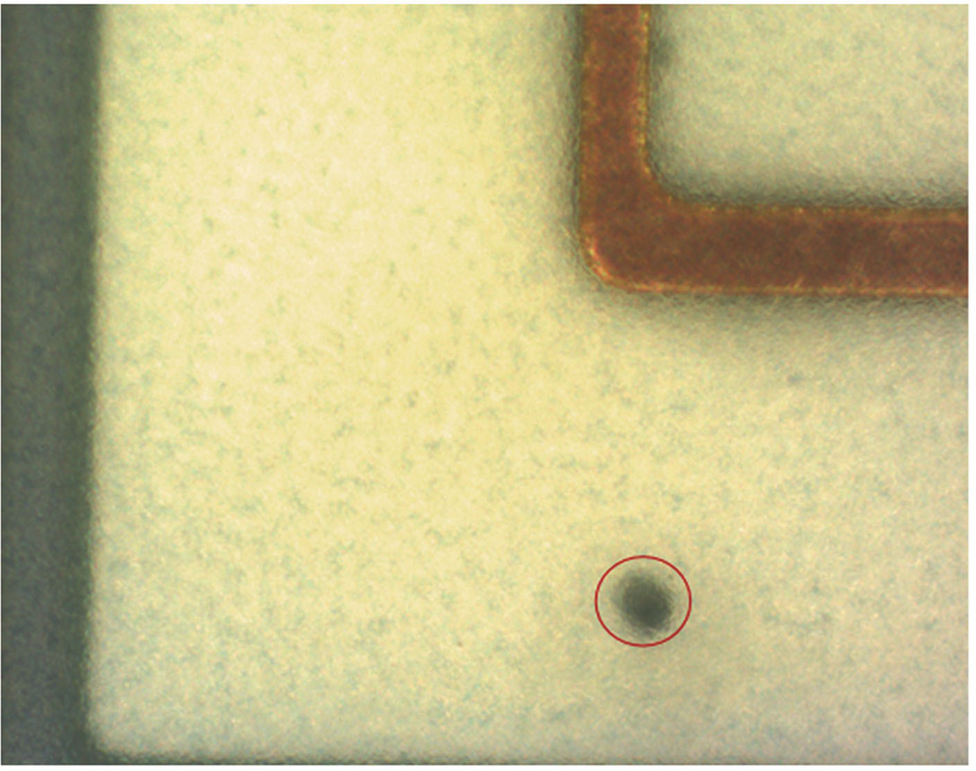
Fig. 1. Optical micrograph of ESD black spot
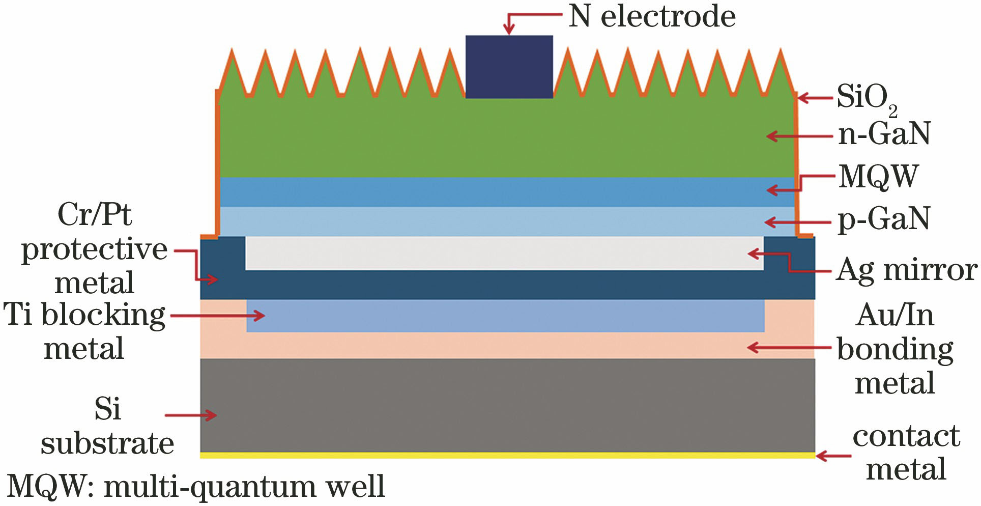
Fig. 2. Schematic of chip structure
Fig. 3. Chip morphologies after application of different ESD voltages. (a) 300 V; (b) 400 V; (c) 600 V; (d) 800 V; (e) 1000 V; (f) SEM image of ESD black spot in Fig.3 (e)
Fig. 4. I-V characteristic curves of LED chip
Fig. 5. Photoluminescence micrographs. (a) Before black spot emerging; (b) after black spot emerging
Fig. 6. EDS component analysis of electro-static breakdown spillage. (a) Electro-static hole measured by EDS; (b) EDS energy spectrum of electro-static breakdown spillage
Fig. 7. SEM images of GaN roughness surface under different EDS voltages. (a) 400 V; (b) 600 V; (c) 800 V; (d) 1200 V; (e) 1500 V
Fig. 8.
SEM image of wafer C3 after FIB etching
|
Table 1. Number of ESD black spots inside and outside electrode line
| |||||||||||||||||||
Table 2. Number of ESD black spots in inner and outer rings of wafer

Set citation alerts for the article
Please enter your email address
© Copyright 2018-2021 | Chinese Laser Press. All Rights Reserved 沪ICP备15018463号-20