
Zhongjie Guo, Ningmei Yu, Longsheng Wu. Column readout circuit with improved offset mismatch and charge sharing for CMOS image sensor[J]. Journal of Semiconductors, 2019, 40(12): 122404
- Journal of Semiconductors
- Vol. 40, Issue 12, 122404 (2019)
Abstract
1. Introduction
Although the charge coupled device (CCD) image sensors have been widely used during the past several decades, complementary metal oxide semiconductor (CMOS) image sensor (CIS) have brought a huge popularity to various imaging applications due to the advantages over CCD image sensor such as system on chip (SOC), low power consumption, and lower cost. The dynamic range and signal-to-noise ratio are two key parameters which determine the performance of an image sensor. In these characteristics, it is obvious to one that the noise parameter is the key technology because the dynamic range is the result of full swing range over the readout noise and the signal-to-noise ratio is the results of signal power over the noise power[
To reduce the temporal noise, high gain column amplifier is adopted in the first stage of the column readout chain[
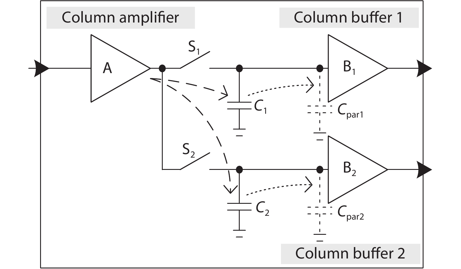
2. Traditional column readout designs
Several CMOS image sensor architectures have been reported according to the types of the signal readout schemes and the position of the analog to digital processing. A typical readout circuit of CMOS image sensor with a noise canceller for fixed pattern noise and reset noise of pixels is shown in Fig. 1. By controlling the timing sequence of switches S1 and S2, the reset level and signal level of the amplified pixel output are sampled on the capacitor C1 and C2 respectively[
![]()
Figure 1.Column readout with two buffers.
Therefore, a serial output through single column buffer was designed to overcome the offset, as shown in Fig. 2[
![]()
Figure 2.Column readout with single buffer.
where V(L1) is the last stage level on the column buffer input Cpar before switch S3 turns on, V(L2) is the last stage level on the column buffer input Cpar before switch S4 turns on. So, V(L1) has an approximate storage value of reset level, V(L2) has an approximate storage value of image level during the last row readout. Although there is a correlation between each adjacent row, but for the low noise demanding, the difference will induce enough performance deteriorating owing to the discharge and fixed pattern noise.
3. Proposed column readout structures
Based on the analysis of traditional column solution, a low noise column readout circuit with improved charge sharing for CMOS image sensor is proposed in this paper, as shown in Fig. 3(a), and the control timing is shown in Fig. 3(b). The presented approach is composed by the column amplifier, reset level storage capacitor C1, image level storage capacitor C2, a single column buffer and eight switches. In the sample phase, firstly the switch S1 which connect the column amplifier and both plates of capacitor C1 is on, the reset level from pixel column line can be sampled on the capacitor C1, as shown in Fig. 4(a). Then the switch S2 which connect the column amplifier and both plates of capacitor C2 is on, the image level from pixel column line can be sampled on the capacitor C2, as shown in Fig. 4(b). In the buffer phase, firstly the switch S3 which connect both plates of capacitor C1 and the column buffer is on, the reset level sampled on the capacitor C1 can be buffered out to the next stage, as shown in Fig. 4(c). Secondly the switch S4 which connect both plates of capacitor C2 and the column buffer is on, the image level sampled on the capacitor C2 can be buffered out to the next stage, as shown in Fig. 4(d). Since the input operating point is unchanged, it can be seen that this method not only adopts a single column buffer to eliminate the offset, but also improves the charge sharing by the bottom plate sampling.
![]()
Figure 3.(a) Proposed column readout. (b) Control timing of the proposed circuit.
![]()
Figure 4.(a) Reset level sample phase. (b) Image level sample phase. (c) Reset level buffer phase. (d) Image level buffer phase.
A large array CMOS image sensor is composed by a great number of column readout circuits. Generally, the sample phase is parallel at same time in a row pixel, and the buffer phase is consecutive to transmit from column 1 to column n. n column readout circuit adopted proposed approach is designed in Fig. 5, where each column readout has two input ports, one is the pixel output, and another is the common voltage VCM, which is shared to all columns, but with enough driving capability, where the maximum load capacity we designed is 10 mA. The detail control timing is shown in Fig. 6.
![]()
Figure 5.
![]()
Figure 6.Control timing of
4. Measurement results
The low noise column readout circuit with improved offset mismatch and charge sharing for CMOS image sensor is implemented in 55 nm CMOS image sensor technology. The die micrograph of the fabricated sensor is shown in Fig. 7, which consists of a 1024 × 1024 pixel array and peripheral circuitry. The column parallel readout circuit is located on a single side below the pixel array. In order to measure the performance of the proposed approach how it improve the offset mismatch and charge sharing, the output gray code variances with exposure time and rms value is measured for all pixels by using a 14 bit ADC. Based on EMVA 1288 presented by European Machine Vision Association, a full set of parameters measurement procedures were done on the test image sensor.
![]()
Figure 1.Column readout with two buffers.
Fig. 8 shows a comparative curve with and without the proposed technique applied to the readout circuit under bright and dark conditions. In contrast to conventional architectures, the proposed architecture achieves an excellent linearity output code versus exposure time, which can be increased by 20%. As we can see that the traditional solution dramatically decreased the linearity under bright field and the nonuniformity under dark field, which will deteriorate the image quality during low light to high light application. Furthermore, Fig. 8 shows the measurement results of the nonuniformity with conventional and proposed approach under bright and dark conditions. The proposed architecture can get optimization uniformity lower than ten digital codes, but the conventional method shows a worse noise and growth rate. As is shown, the photo response nonuniformity is reduced by 40% and 30% in bright and dark field. Because the parasitic capacitor can’t be matched in the readout chain, the proposed approach without parasitic influence will provide an excellent uniformity. It is verified significantly by the prototype sensor chip, and the statistics results show a better PRNU less than 1.16%. Finally, the comparison of actual image before and after the optimization is shown in Fig. 9. In order to improve the recognition, we extracted part of the image, where the resolution of the pixels shown in the picture is about 10 × 10, and performance summary and comparison with the state of the art are given in Table 1.
![]()
Figure 2.Column readout with single buffer.
![]()
Figure 1.Column readout with two buffers.
Table Infomation Is Not Enable5. Conclusions
With the pixel array resolution increasing, the column parallel readout topology is facing the challenges in high speed, high accuracy and low noise application. The reset level and the image level of the storage capacitor are sampled by the correlated double sampling technology in the traditional method. However, the offset mismatch which is introduced in the two buffers is not certain related to the luminance of light, and it can’t be cancelled by the CDS because of the intrinsic unbalanced structure and the electrical properties. Due to the difference between the sequential rows, the charge sharing exists in the image level point evidently, and it also exists in the reset level point which is induced by fixed pattern noise. However, the charge sharing which exists in the single buffer structure can result in the charge exchange between the reset level and image level which is critical to the readout noise. Therefore, column readout circuit with improved offset mismatch and charge sharing using a single buffer with eight switches is proposed in this paper. The key technology presented in our design not only avoids the charge sharing through the extra switches, but also keeps the constant operating point, which is favorable to the low noise design. A 1024 × 1024 pixels CMOS image sensor including 1024 columns readout has been fabricated in a 55 nm 1P4M CMOS with pinned photodiode process. The measurement results show that the linear range is extended by 20%, the readout noise is reduced by 40% and 30% in bright and dark field, and the photo response nonuniformity is up to 1.16%. Finally, a raw sample image taken by the prototype sensor shows the excellent practical performance.
Acknowledgments
This work was supported by Shaanxi Education Department (No. 19JC029).
References
[1] A Boukhayma, A Peizerat, C Enz. Temporal readout noise analysis and reduction techniques for low-light CMOS image sensors. IEEE Trans Electron Devices, 63, 72(2016).
[2] N Kawai, S Kawahito. Noise analysis of high-gain, low-noise column readout circuits for CMOS image sensors. IEEE Trans Electron Devices, 51, 185(2004).
[3] S F Yeh, K Y Chou, H Y Tu et al. A 0.66erms- temporal-readout-noise 3-D-stacked CMOS image sensor with conditional correlated multiple sampling technique. IEEE J Solid-State Circuits, 53, 527(2018).
[4] Y Lim, K Koh, K Kim et al. A 1.1e- temporal noise 1/3.2-inch 8 Mpixel CMOS image sensor using pseudo-multiple sampling. IEEE Int Solid-State Circuits Conf Dig Tech Papers (ISSCC), 396(2010).
[5] M W Seo, S Suh, T Lida et al. An 80 μV rms-temporal-noise 82 dB-dynamic-range CMOS image sensor with a 13-to-19 b variable-resolution column-parallel folding-integration/cyclic ADC. IEEE Int Solid-State Circuits Conf Dig Tech Papers (ISSCC), 400(2011).
[6] N Chen, S Y Zhong, M Zou et al. A low-noise CMOS image sensor with digital correlated multiple sampling. IEEE Trans Circuits Syst I, 65, 84(2018).
[7] Q Y Liu, A Edward, M Kinyua et al. A low-power digitizer for back-illuminated 3-D-stacked CMOS image sensor readout with passing window and double auto-zeroing techniques. IEEE J Solid-State Circuits, 52, 1591(2017).
[8] K Kawahito. Signal processing architectures for low-noise high-resolution CMOS image sensors. IEEE Custom Intergrated Circuits Conference (CICC)(2007).
[9] S Okura, O Nishikido, Y Sadanaga et al. A 3.7 M-pixel 1300-fps CMOS image sensor with 5.0 G-pixel/s high-speed readout circuit. IEEE J Solid-State Circuits, 50, 1016(2015).
[10] T Watabe, K Kitamura, T Sawamoto et al. A 33M pixel 120fps CMOS image sensor using 12b column-parallel pipelined cyclic ADCs. IEEE Int Solid-State Circuits Conf (ISSCC) Dig Tech Papers, 388(2012).


Set citation alerts for the article
Please enter your email address

© Copyright 2018-2021 | Chinese Laser Press. All Rights Reserved 沪ICP备15018463号-20