Tiecheng Wang, Xiangdong Zhang. Improved third-order nonlinear effect in graphene based on bound states in the continuum[J]. Photonics Research, 2017, 5(6): 629
Copy Citation Text
The scattering matrix theory has been developed to calculate the third-order nonlinear effect in sphere-graphene-slab structures. By designing structural parameters, we have demonstrated that the incident electromagnetic wave can be well confined in the graphene in these structures due to the formation of a bound state in the continuum (BIC) of radiation modes. Based on such a bound state, third-harmonic (TH) generation and four-wave mixing (FWM) have been studied. It is found that the efficiency of TH generation in monolayer graphene can be enhanced about 7 orders of magnitude. It is interesting that we can design structure parameters to make all beams (the pump beam, probe beam, and generated FWM signal) be BICs at the same time. In such a case, the efficiency of FWM in monolayer graphene can be enhanced about 9 orders of magnitude. Both the TH and FWM signals are sensitive to the wavelength, and possess high Q factors, which exhibit very good monochromaticity. By taking suitable BICs, the selective generation of TH and FWM signals for S- and P-polarized waves can also be realized, which is beneficial for the design of optical devices.
In recent years, nonlinear optical properties of graphene have attracted much attention because recent investigations have shown that the third-order nonlinear optical response of the single-atom-layer graphene is particularly strong [1–5]. Many studies have focused on such an aspect, such as saturable absorption [6–11], optical limiting [12,13], two-photon absorption [14], four-wave mixing (FWM) [1,15,16], and third-harmonic (TH) generation [17–24]. This allows one to employ graphene in active photonic devices with improved functionality [3,18,19]. In these applications, the strength of interaction between graphene and electromagnetic (EM) waves plays a central role. In general, such an interaction is weak due to the single atom thickness of graphene. The weak interactions block efficient generation of nonlinear effects and potential applications of graphene in optoelectronic devices. Thus, various methods to improve the interaction between graphene and EM waves have been proposed [5–13,25–27]. For example, TH generation may be dramatically enhanced in monolayer graphene by inserting it in properly designed 1D photonic crystals (PCs) [28] or using ultrastrong localized surface plasmon resonances [29–31].
On the other hand, analogous to the localized electrons with energy larger than their potential barriers, light bound states in the continuum (BIC) have been observed experimentally in recent years [32–34]. The BICs are known as embedded trapped modes, which correspond to discrete eigenvalues coexisting with extended modes of a continuous spectrum [35–37]. For example, the BICs for the EM wave have been shown to exist in the dielectric gratings [35], waveguide structures [32,36,38–40], the surface of the object [37,41], PC slabs [33,34,42,43], and some open subwavelength nanostructures [44–46]. Photonic nanostructures with such BICs possess many advantages. First, they may be more easily implemented compared with the electron system. In the electronic quantum system, some artificially designed potentials cannot be readily realized. Second, they may have a variety of potential applications, such as biosensing, perfect filters, and so on.
Motivated by these investigations, in this work we explore the possibility to improve the efficiency of the third-order nonlinear effect in graphene using BICs. Two kinds of third-order nonlinear effect, TH generation and FWM, are considered. The method to calculate these nonlinear effects in sphere-graphene-slab structures and multilayer structures has been developed. We find that the efficiency of the TH generation and FWM can be dramatically enhanced in monolayer graphene based on BICs. The generated signals possess very good monochromaticity. The physical origin for such a phenomenon has also been analyzed. The rest of this paper is organized as follows: We will describe the theory and method in Section 2, present the results and discussions in Section 3, and give a summary in Section 4.
Sign up for Photonics Research TOC. Get the latest issue of Photonics Research delivered right to you!Sign up now
2. THEORY AND METHOD
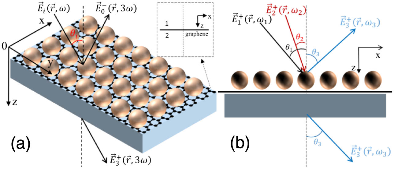
We consider a three-layer structure consisting of monolayer dielectric spheres with a square lattice, a monolayer graphene, and a dielectric slab, as shown in Figs. 1(a) and 1(b); the monolayer graphene is placed at the interface between the monolayer dielectric spheres and the dielectric slab. The distance between two neighbor spheres is taken as , the radius, relative permittivity, and relative permeability of spheres are denoted by , , and , respectively; the spheres are immersed in the air. The thickness, relative permittivity, and relative permeability of the dielectric slab are represented by , , and , respectively. All these materials are taken to be nonmagnetic . The thickness, conductivity, and third-order susceptibility of the monolayer graphene are marked by , , and ; the nonlinear surface current due to the third-order nonlinear effects of the monolayer graphene at the graphene location is , where and represent the angular frequency of the TH EM wave and the third-order polarization density.
Figure 1.(a) Diagram of the sphere-graphene-slab structure and the TH generation process. The spheres are arranged in a square lattice with lattice constant ; the thickness of the dielectric slab is , and the monolayer graphene is put at the interface between the monolayer dielectric spheres and the dielectric slab. When a plane wave with angular frequency is incident on the structure at the incident angle , the transmitted and reflected TH fields are generated due to the third-order nonlinear effect of graphene. Inset shows graphene layer with up medium denoted by 1 and down medium marked by 2. (b) Schematic of the degenerate FWM process in the three-layer structure. The pump beam at frequency and the probe beam at frequency are incident on the structure with arbitrary incident angles and . Because of the third nonlinear effect of the graphene, the transmitted and reflected beams at FWM frequency are generated with angle . The angle is determined by the in-plane phase-matching condition.
The surface conductivity of the graphene is governed by the Kubo formula [47–54]; we take the conductivity as follows:
The surface conductivity contains the intraband contribution and the interband contribution ; here, , , , and are the electronic charge, Planck constant, Boltzmann constant, and temperature, respectively; , , and represent the Fermi distribution, Fermi energy, and relaxation rate. We take the temperature and relaxation rate as and [55] in the following calculation. In the THz regime, when and , the conductivity of graphene can be well approximated by the Drude-like expression [56], where is the well-known universal conductivity. Thus, the conductivity can be tuned by changing the Fermi level via chemical doping or applying a gate voltage.
Based on the recent theoretical and experimental studies, the only nonzero components of the third-order susceptibility tensor are , , and due to the isotropic nature. We assume and neglect for [19] and take the susceptibility as [20,21] compatible with the recent study. When the irradiance on graphene is increased, the saturation effect [57] will be enhanced; the third-order susceptibility is modified and taken as , where is the saturation coefficient [58,59], and are the electric field on graphene. The saturation field is taken from the experimental data [58]. In the following, we will provide the calculation method for TH generation and FWM in such a structure.
A. Theory for the TH Generation in the Sphere-Graphene-Slab Structure
When a plane wave with angular frequency is incident on the structure at the incident angle , as shown in Fig. 1(a), the transmitted and reflected TH fields are generated due to the third-order nonlinear effect of graphene. The fundamental frequency (FF) field [, , and ] can be calculated by the layer-multiple-scattering method, of which details of the calculation process are described in Ref. [60]. Thus, the third-order polarization densities of graphene are expressed as , , and ; here, and represent and components of the FF electric field on the graphene, which is located at the interface ; the corresponding surface currents are expressed as and .
In the following, we present the calculated method for the TH generation in such a structure. Because the sphere layer and dielectric slab are considered as the linear materials, at the TH frequency we only consider the scattering matrix of graphene. We first consider that a monolayer graphene laid at the interface , as shown in inset of Fig. 1(a), is radiated by a plane wave at the FF from the plane; the up/down medium of the graphene is denoted by 1/2. The TH electric and magnetic fields at the up/down medium of the graphene are marked by and with and components of the wave vector marked by and ( and ), the components of the wave vector in the up and down media are equal. At the boundary, we have where represents the direction of the normal unit vector at the interface. The electric fields at the TH frequency in the up and down media can be expressed as
Here , , and represent the expanded coefficients of the electric TH fields. Inserting Eq. (5) into the boundary condition Eq. (4), we obtain the relations between the electric fields up and down the graphene: where and represent the transmission coefficients, and and are reflection coefficients, which are given by
Here , , , and are the nonlinear terms originating from the third-order nonlinear effect of graphene and are expressed as where and are the permittivity and permeability of the vacuum, respectively. In the following, we extend the layer-multiple-scattering method to include a nonlinear graphene layer. The electric fields outside the graphene layer are expressed as , , and , which represent the incident wave along the direction (propagating downward) and the corresponding transmitted wave along direction and reflected waves along direction (propagating upward). The corresponding waves with opposite directions are marked by , , and , respectively. These waves can be expanded as a set of plane waves: where represent the , coordinates; is the Bragg wave vector and . Here, is the wave vector, and is the reduced wave vector, which lies in the surface Brillouin zone; is the general reciprocal vector, and and represent the reciprocal lattice vector. Outside the graphene, the relationships between the incident and the transmitted (reflected) waves are where denotes a wave propagating downward (upward); the matrixes and are given by where is the azimuthal angle of with respect to the axis and is the parallel component of . Here , , , and represent the elements in matrixes ; , , , and are the elements in matrixes . We can further calculate scattering matrixes and for the monolayer graphene, the subscript number 2 in these matrixes denotes the graphene layer (because it is the second layer in the structure). Similarly, we can also obtain and (the scattering matrixes of the spheres layer), and (the scattering matrixes of the dielectric layer). The incident fields from two sides of graphene can be expanded in plane waves and , the output fields and from two sides of graphene can be expanded in a similar way; here , , , and . Then the electrical fields outside the graphene can be expressed as where the electrical fields up and down the graphene are written in the matrix forms and ; here, the superscript represents matrix transposition. In a similar way, the electric fields up the sphere layer and down the dielectric layer can also be expanded in plane waves and ; we also define the corresponding matrixes and .
In the following, we attempt to calculate the scattering matrixes of the three-layer structure, which are marked by and based on the scattering matrixes of every layer. First, we calculate the scattering matrixes of the first two successive layers (the spheres layer and graphene layer), which are denoted by and . The matrixes and can be obtained by combining the matrixes and of the sphere layer and the matrixes and of the graphene layer: where the matrixes in Eq. (13) are consistent with those in Ref. [60]; are the corresponding nonlinear terms, which are provided for the first time. Then, in a similar way with that given above, we can obtain the scattering matrixes and of the three successive layers based on the scattering matrixes and of the first two successive layers and the scattering matrixes and of the dielectric layer. Thus, we can obtain the TH fields upside and downside the three-layer structure from the following relation:
Based on the calculated TH fields in Eq. (15), the electric field intensities of the transmitted and reflected TH fields radiated from the three-layer structure can be calculated by
The electric field intensity of the incident FF field can also be calculated based on the known incident FF electric field ; it is
In the calculating the sums of Eq. (16) waves with imaginary component of wave vector (decaying waves) are dropped, as they do not transfer energy along the direction.
Then, the conversion efficiencies for the transmitted (F1), reflected (F2), and total (F3) TH fields can be obtained:
In order to compare the TH fields generated in the three-layer structure with those in the freestanding graphene, the enhancements of the transmitted (G1), reflected (G2), and total (G3) TH field are introduced as where and represent the electric field intensities of the transmitted and reflected TH fields generated in the freestanding graphene. Based on the above relations, we can obtain the conversion efficiencies and the enhancements for TH fields using numerical calculations.
B. Theory for the FWM in the Sphere-Graphene-Slab Structure
Now we turn to the FWM of the three-layer structure shown in Fig. 1(b). This structure is illuminated by a pump beam at frequency and incident angle ; it is also radiated by a probe beam at frequency and incident angle . Due to the third-order effect of the graphene, the transmitted beam and reflected beam at the FWM frequency are generated; here, the subscripts 1, 2, and 3 represent the three waves. The fields for them are expressed as where the symbols shown in Eq. (19) represent the positive (negative) real parts of the components of the wave vector. If three frequencies are not equal, the nonlinear polarization along the direction on the graphene can be expressed as
In the same way, the nonlinear polarization along the direction, , can also be obtained. The directions of the transmitted and reflected FWM waves are determined by the in-plane phase-matching condition: . For example, we consider a particular case that all the frequencies (the pump, probe, and FWM waves) are equal, that is, . In such a case, if the pump wave is incident normally (), the angles of the probe and FWM waves are equal () due to the phase-matching condition, the transmitted and reflected FWM fields are optical phase conjugations. By considering the terms that have the same transverse momentum, we divide the third-order nonlinear polarization densities on the graphene along the direction into three parts, i.e., , , and : with
The corresponding , , and can be obtained in the same way; all the electrical fields here are taken on the graphene. The first terms in Eq. (21) represent a phenomenon called self-phase modulation [61,62], which results from dipole excitations induced by three photons, the second and third terms correspond to cross-phase modulation, the fourth terms lead to the generation of the optical phase conjugations. After the third-order nonlinear polarization densities are calculated, the surface currents of the graphene, and , can be obtained. Similar to the method for the TH generation shown in previous part, the scattering matrixes in the present case can also be obtained; the field intensities for the transmitted () and reflected () FWM waves can be obtained through numerical calculations. Furthermore, we can calculate the transmission and reflection coefficients, and , to characterize the efficiencies of FWM generations:
Here, represent the intensities of the incident probe beams.
3. RESULTS AND DISCUSSIONS
In this section, we present numerical results for the TH generation and FWM from the three-layer structures. The dielectric constants of spheres are taken as 6.25, which correspond to thallium iodide [63]. The lattice constant is taken as . We take [64] as the dielectric slab, the corresponding dielectric constant is taken as [64]; here , , , , and . The radius of the sphere and the thickness of the dielectric slab are designed as and , respectively. The third-order nonlinear effects of the spheres and dielectric slab are neglected.
An important feature is that the BICs around the graphene layer are easy to appear in these three-layer structures, which has been discussed in the previous investigation [43]. In Fig. 2(a), we plot the electric field intensities at the interface (graphene layer) between the sphere and the slab for and . Here the P-polarized incident wave with the intensity is radiated to the plane of the sample with , P- or S-polarized wave represents the TM or TE mode. The field localizations are observed at different wavelengths due to the formation of bound states. These BICs lead to the appearance of the resonant absorption. Figure 2(b) displays the corresponding results of the absorption as a function of wavelength. It can be seen clearly that the resonant absorption reaches 67% at when the Fermi energy is taken as 0.23 eV, while the absorption peak is only 2.7% at when the Fermi energy is 0.7 eV. This is because the imaginary part of the conductivity of graphene is small (near zero) at , which can be seen from the inset of Fig. 2(a). From the inset in Fig. 2(a), we can also see that and correspond to two variation characteristics of the graphene conductivity. In the following, we study the generation signals for the TH and FWM waves based on these BICs.
Figure 2.(a) The absorption as a function of the wavelength when the Fermi energy is taken as (black line) and (red line). Inset shows the conductivity of the graphene. (b) The electric field distribution at the graphene location below the bottom of the spheres when the Fermi energy is taken as (black line) and (red line).
A. Numerical Results for the TH Generation Based on BICs
In Fig. 3(a), we plot the TH conversion efficiency from the structure shown in Fig. 1(a) as a function of the FF wavelength at . The corresponding results at are shown in Fig. 3(b). Here the intensity and incident angle of the pump P-polarized beam are taken as and 5°, which corresponds to the case in Fig. 2. For comparison, the TH conversion efficiencies of the monolayer graphene in vacuum are also plotted in Figs. 3(a) and 3(b). Because of the mirror symmetry of the freestanding monolayer graphene, the corresponding conversion efficiencies of F1 and F2 are nearly equal, so the black and red dashed lines coincide with each other.
Figure 3.Transmitted (F1), reflected (F2), and total (F3) TH conversions in the three-layer structure and freestanding graphene as a function of the FF wavelength when the Fermi energy is taken as (a) and (b) . The TH enhancement G3 of TH signal in the three-layer structure compared with that in the freestanding graphene as a function of the FF wavelength for (c) different radius of the spheres or (d) various thickness of the slab, the Fermi energy in (c) and (d) is taken as .
The total TH conversion efficiency F3 reaches at the wavelength 1824.91 nm for and at the wavelength 1824.51 nm for due to the improved field localizations from BICs. The corresponding TH signals are enhanced about 5 and 7 orders of magnitude at two cases, respectively, as compared with the bare monolayer graphene. The efficiency of the forward optical phase conjugate wave and backward optical phase conjugate wave is nearly equal [16]. The calculations in Ref. [28] have shown that the TH generation can be enhanced 5 orders of magnitude using the defect in 1D PC. However, for such a way, the sample with dozens of layers has to be fabricated. Instead, only three layers are needed in our structure.
In addition to the high efficiency, the signals generated in this way have good monochromaticity due to high factors of bound states. The monochromaticity can be described by the relative linewidth in the signal spectrum; here is the center wavelength of the peak and represents full width at half maximum (FWHM) of the peak. From Figs. 3(a) and 3(b), we obtain that are 0.0356% and 0.0175% for the cases with and , respectively, which is much less than the relative linewidth (about 1% in Ref. [65]). This means that the TH conversion efficiency is low when the frequency is taken at the deviation of the BICs. For example, at 1822 nm the TH conversion in the three-layer structure is nearly as large as that in the freestanding graphene; at the 1815 nm, the TH conversion in the three-layer structure is 2 orders of magnitude smaller than that in the freestanding graphene.
Figures 3(c) and 3(d) display the calculated results of the TH enhancement G3 as a function of the FF wavelength for different radius of the spheres and various thickness of the slab. The other parameters are identical with those in Fig. 3(a). It is clearly seen from Fig. 3(c) that the peak of G3 is slightly redshifted with the increase of the radius of the spheres. In Fig. 3(d) the peak of G3 is redshifted obviously with the increase of the thickness of the slab. We can utilize this property to tune the peak location of the TH signal by changing the thickness of the slab.
The above discussions are only for a fixed incident angle of the incident wave. In fact, the phenomena strongly depend on the incident angle of the wave. Figure 4 shows the calculated results for the TH enhancement as functions of the FF wavelength and the incident angle at . Here, the intensity of the pump beam is taken as . Figures 4(a) and 4(b) correspond to the transmitted enhancement for the S- and P-polarized pump beams, respectively; the corresponding results for the reflected enhancement are given in Figs. 4(c) and 4(d). It is seen clearly that both G1 and G2 are sensitive to the incident angle. There are common TH enhancement peaks around the wavelength 1825.57 nm for S- and P-polarized pump beams located at the normal incident angle.
Figure 4.TH enhancement of the (a) and (b) transmitted and (c) and (d) reflected TH beams as a function of the fundamental wavelength and the incident angle for S-(P) polarized pump beam. (e) and (f) show the absorption spectra of the three-layer structure. The bound states are denoted by S1, S2, and S3 (P1 and P2) for S-(P) polarized wave.
With the increase of the incident angle from 0° to 30°, the peaks split into three for the S-polarized pump beam (S1, S2, and S3) and do not split for the P-polarized pump beam (P1). At the same time, we find that S2 and P1 overlap each other, which are blueshifted with the increase of the incident angle. These phenomena originated from the formation of BICs. This can be seen clearly in Figs. 4(e) and 4(f), which display the corresponding absorptions as functions of the wavelength and the incident angle of the incident wave for S- and P-polarized waves, respectively. The angle-dependent resonant absorptions are clearly visible in Figs. 4(e) and 4(f) corresponding to the existence of trapped EM modes (BICs) in the structure. The change characters of angle-dependent BICs are analogous to those of TH generations, as shown in Figs. 4(a)–4(d). This means that the formation of BICs leads to angle dependences of TH generations.
B. Numerical Results for the FWM Based on BICs
For the FWM from the structure shown in Fig. 1(b), we consider two kinds of cases: Case I and Case II. For Case I, the waves keep the same frequency in the process, as shown in Fig. 5(a), while the waves are in different frequencies for Case II. For Case I, the FWM from bare graphene has been discussed in Ref. [15]. In Fig. 5, we present the comparison between our results with those from the bare graphene; here, the wavelengths are denoted by .
Figure 5.(a) Schematic of the FWM progress in the three-layer structure when all the waves are at the same wavelength; the incident angles of the pump and probe beams are 0° and , respectively; the angle of the generated FWM wave is equal to because of phase-match condition. (b) and (c) correspond to and of the transmitted and reflected FWM beams as a function of the FF wavelength and incident angle of the probe beam. The and in the three-layer structure and freestanding graphene as a function of the fundamental wavelength at corresponding to the maxima when the Fermi energy is taken as (d) and (e) . The blue and pink lines show the absorption spectra under only one incident beam at the incident angles and , respectively.
Figures 5(b) and 5(c) show the transmission () and reflection () of the generated FWM signals as functions of the wavelength and the angle of the probe beam at . Here the P-polarized waves are used as the probe and pump beams; the intensities of the pump and probe beams are taken as and . These intensities lead to a negligible saturation effect of the graphene. We can see that three resonant peaks (denoted by 1, 2, and 3) appear in Figs. 5(b) and 5(c), respectively; these phenomena are originated from the formation of BICs of the pump and probe beams in this structure. The resonant modes 1 and 2 correspond to the resonant modes P1 and P2, as shown in Fig. 4(f); the vertical resonant mode 3 corresponds to the BIC of the pump beam with the normal incident angle. When all beams are in BICs, the maxima of the generated FWM signals can be obtained, as shown by bright dots in Figs. 5(b) and 5(c). This can be seen more clearly in Fig. 5(d).
In Fig. 5(d), we plot the transmission (black lines) and the reflection (black triangle lines) as a function of the wavelength . Here, the incident angle of the probe beam is fixed at ; the other parameters are identical to those in Figs. 5(b) and 5(c), where a resonant peak [corresponding to the red point in Fig. 5(b)] around appears. In order to understand this phenomenon, we also plot the corresponding absorption spectra; the blue line corresponds to the absorption when the beam irradiates the structure with the normal incident angle; the pink line corresponds to the absorption spectrum, where the incident angle is taken as 16.09°. We can see that two absorption peaks for two cases correspond to the resonant peaks for the generated FWM signals, which also correspond to two BICs for the pump and probe beams. When the pump and probe beams are located at the BICs, the corresponding EM fields are localized at the graphene layer, and then the corresponding third-order polarization densities are largely enhanced. This is the reason why we can observe enhancement of FWM signals about 6 orders of magnitude around the resonant peak at . The relative linewidth of the resonant peak is 0.0346%, which means that good monochromaticity of the generated signal is observed again.
After the Fermi energy is tuned to , while other parameters are not changed, the corresponding results are shown in Fig. 5(e). In such a case, the FWM signal is enhanced about 9 orders of magnitude around the resonant peak, and the relative linewidth of the resonant peak reaches 0.00863%. This is because of small imaginary part and low loss of absorption, which corresponds to strong localization of the electric field, as described in Fig. 2(a).
For the bare graphene, the previous investigation has shown that the optical phase conjugation can be tuned in a large range by changing the phase difference [16]. In fact, the present structure still possesses such a property. The solid lines and dashed lines in Fig. 6 represent the transmission and reflection of the optical phase conjugations as a function of the phase difference between the two parts of the pump beam (the pump beam is divided into two parts with the same intensity ). The intensity and incident angle of the probe beam are taken as and 16.09°, respectively; the other parameters taken here correspond to the maximum in Fig. 5(c). A period modulation in the generation of optical phase conjugations is clearly observed; a maximum is reached when the phase difference is equal to 0°. A minimum appears when the phase difference is equal to 180°; the period is 360°. This phenomenon is similar to that in Ref. [16]; that is, we can also tune the optical phase conjugation in a large range by changing the phase difference in the present case.
Figure 6.Transmission () and reflection () as a function of the phase difference between the two parts of the pump beam with the same intensity.
For Case II, as shown in Fig. 7(a), we consider a pump beam normal to the surface of the structure at the wavelength and a probe beam with an incident angle and the wavelength . Due to the third-order nonlinear effect of the graphene, the transmitted and reflected FWM signals at the angle and wavelength are generated. In this process, the following relations are satisfied:
Figure 7.(a) Schematic of the FWM progress in the three-layer structure when the wavelengths of the pump and probe beams ( and ) are not equal, the incident angles of the pump and probe beams are and , respectively. (b) and (c) correspond to the transmitted and reflected FWM beams as a function of the wavelength and incident angle of the probe beam. The wavelength of the probe beam is taken as .
Figures 7(b) and 7(c) display and of the generated FWM signals as a function of the wavelength of the pump beam and the angle of the probe beam ; the wavelength of the probe beam is taken as . The intensities of the pump and probe beams are taken as and ; the Fermi energy is . It is seen clearly that there are two vertical resonant modes (at and ) in every figure, which correspond to two BICs of the normal pump beam.
When the angles of the probe beam are taken as and , the probe beam is also in BICs. In such a case, strong FWM signals at (Point A) and (Point B) are generated [see bright dots in Figs. 7(b) and 7(c)]; the corresponding wavelength for these signals is . Points A and B are highlighted because the probe beam, pump beam, and generated FWM signal at these points are in BICs simultaneously; in such a case, very high generated efficiency can be obtained. The generated efficiency at point A is even more prominent because of the better electric field confinement of the probe beam. These can be seen more clearly in Fig. 8.
Figure 8. and in the three-layer structure and freestanding graphene as a function of the wavelength with , which correspond to a peak when the Fermi energy is taken as (a) and (c) , respectively. (b) Blue and pink lines show the absorption as a function of the wavelengths of the pump or FWM beams ( or ) under one incident beam at the incident angles 0° and , respectively; the two relations are put together via phase match condition.
In Fig. 8(a), we plot and as a function of at and , which corresponds to the maxima in Figs. 7(a) and 7(b). The other parameters are identical with those in Figs. 7(a) and 7(b). It is clearly seen that two peaks appear, which are located at and . In order to clearly analyze the origin, in Fig. 8(b) we show the corresponding absorption spectrum of the pump beam (see blue line); two resonant peaks in the absorption spectrum correspond to those shown in Fig. 8(a). Furthermore, we also show the absorption spectrum of the generated FWM signal as a function of (see red line). The resonant absorption peak appears around , which corresponds to . This means that the pump, probe, and FWM beams are located at BICs simultaneously in such a case, which leads to the enhancement of the generated FMW signal about 6 orders of magnitude. This is in contrast with the other cases; for example, the FWM signal is enhanced by about 2 orders of magnitude at because the pump beam is only in the BIC. When the Fermi energy is tuned to , the similar phenomena are observed; the corresponding results are shown in Fig. 8(c). Due to low loss and strong field localization, in such a case the FWM signal is enhanced by about 9 orders of magnitude at compared with that in the freestanding monolayer graphene; the relative line width of the corresponding resonant peak also reaches 0.0195%. The generation efficiency without the enhancement of BICs of the pump and FWM beams is shown away from the peaks in Figs. 8(a) and 8(c); it can be clearly seen that, at , the generation efficiency in the three-layer structure is nearly as large as that in the freestanding graphene; at , the generation efficiency in the three-layer structure is about 2 orders of magnitude smaller than that in the freestanding graphene.
We would like to point out that the purpose of the present paper is to provide theoretical proof of improved third-order nonlinear effect in graphene based on BICs. However, it is more convincing if the experimental observation can be provided. In fact, it is difficult to control the periodic pattern of the nanospheres; we have to optimize the structural design further so that the samples can be fabricated experimentally. These will be our next tasks.
4. SUMMARY
In summary, we have designed sphere-graphene-slab structures to improve the third-order nonlinear interaction between the EM wave and the graphene. The scattering matrix theory to calculate third-order nonlinear effects in these structures has been developed. Improved TH generation and FWM signals from the graphene in these structures has been discussed. Due to the field localization of the BICs, we have found that the efficiency of TH generation from the monolayer graphene in these structures can be enhanced about 7 orders of magnitude compared with that in bare graphene. By designing structure parameters, we can make all beams (the pump beam, probe beam, and generated FWM signal) be BICs at the same time. In such a case, the efficiency of FWM in the monolayer graphene can be enhanced about 9 orders of magnitude. It is interesting that the generated TH and FWM signals possess very good monochromaticity due to the high factors of BICs, which are also sensitive to the incident angle of the wave. Furthermore, we can also obtain selective generations of TH and FWM signals for two polarized waves (S and P waves) by taking suitable BICs. The phenomena can appear at any wavelength from the mid-infrared to far-infrared band, which are very beneficial for the design of optical devices.
[23] J. L. Cheng, N. Vermeulen, J. E. Sipe. Third-order nonlinearity of graphene: effects of phenomenological relaxation and finite temperature. Phys. Rev. B (erratum), 93, 039904(2016).
Tiecheng Wang, Xiangdong Zhang. Improved third-order nonlinear effect in graphene based on bound states in the continuum[J]. Photonics Research, 2017, 5(6): 629