• Photonics Research
  • Vol. 6, Issue 2, 99 (2018)
Daquan Yang1、2、†, Fei Gao3、†, Qi-Tao Cao3, Chuan Wang2, Yuefeng Ji1、2, and Yun-Feng Xiao3、4、*
Author Affiliations
  • 1School of Information and Communication Engineering, Beijing University of Posts and Telecommunications, Beijing 100876, China
  • 2State Key Laboratory of Information Photonics and Optical Communications, Beijing University of Posts and Telecommunications, Beijing 100876, China
  • 3State Key Laboratory for Mesoscopic Physics, School of Physics, Peking University, Collaborative Innovation Center of Quantum Matter, Beijing 100871, China
  • 4Collaborative Innovation Center of Extreme Optics, Shanxi University, Taiyuan, Shanxi 030006, China
  • show less
    DOI: 10.1364/PRJ.6.000099 Cite this Article Set citation alerts
    Daquan Yang, Fei Gao, Qi-Tao Cao, Chuan Wang, Yuefeng Ji, Yun-Feng Xiao. Single nanoparticle trapping based on on-chip nanoslotted nanobeam cavities[J]. Photonics Research, 2018, 6(2): 99 Copy Citation Text show less
    (a) Schematic of the theoretical analysis model, which is a symmetric mirror/microcavity/mirror system. (b) Schematic of a nanoslotted-1D-PC nanobeam cavity for optical trapping. The structure is symmetric with respect to its center (blue dashed line). The trapped nanoparticle is shown within the slot. (c) Calculated Ey distribution (top view with z=0) of the fundamental resonant mode in the microcavity. (d) Ey profile along the centerline of the cavity in the x-direction. The units of the x/y-axis are micrometers (μm). (e) Optical trapping force F distribution profile and (f) trapping potential U distribution profile along the centerline of the cavity in the x-direction (solid line) and fitted Gaussian envelope function (dashed line), respectively, where a=560 nm, wnb=650 nm, h=220 nm, wslot=60 nm, rcenter=0.42a, rend=0.36a, Nt=20, and Nm=5 are chosen.
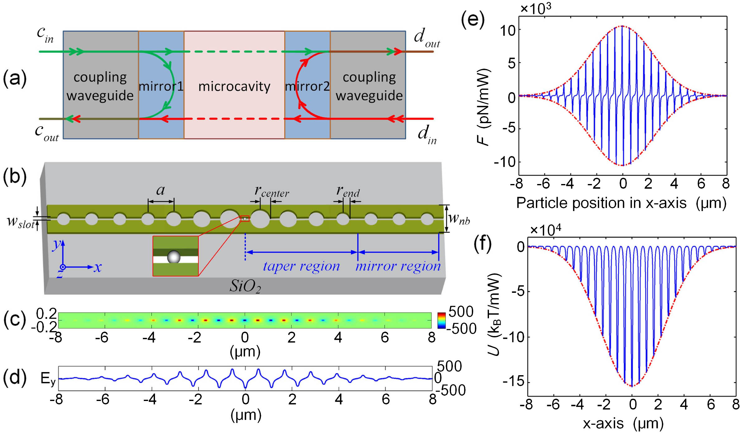
    Fig. 1. (a) Schematic of the theoretical analysis model, which is a symmetric mirror/microcavity/mirror system. (b) Schematic of a nanoslotted-1D-PC nanobeam cavity for optical trapping. The structure is symmetric with respect to its center (blue dashed line). The trapped nanoparticle is shown within the slot. (c) Calculated Ey distribution (top view with z=0) of the fundamental resonant mode in the microcavity. (d) Ey profile along the centerline of the cavity in the x-direction. The units of the x/y-axis are micrometers (μm). (e) Optical trapping force F distribution profile and (f) trapping potential U distribution profile along the centerline of the cavity in the x-direction (solid line) and fitted Gaussian envelope function (dashed line), respectively, where a=560  nm, wnb=650  nm, h=220  nm, wslot=60  nm, rcenter=0.42a, rend=0.36a, Nt=20, and Nm=5 are chosen.
    Influence of different slot widths on (a) cavity transmissivity Tc and Q/V, (b) maximum optical trapping force F and trapping potential U on a 10 nm radius PS nanoparticle, and (c) electric field Ey distributions (top view) taken at the center of the silicon layer (z=0) when wslot is changed from 0 to 200 nm and other parameters are kept fixed as wnb=650 nm, h=220 nm, a=560 nm, rcenter=0.42a, rend=0.36a, Nt=20, and Nm=10.
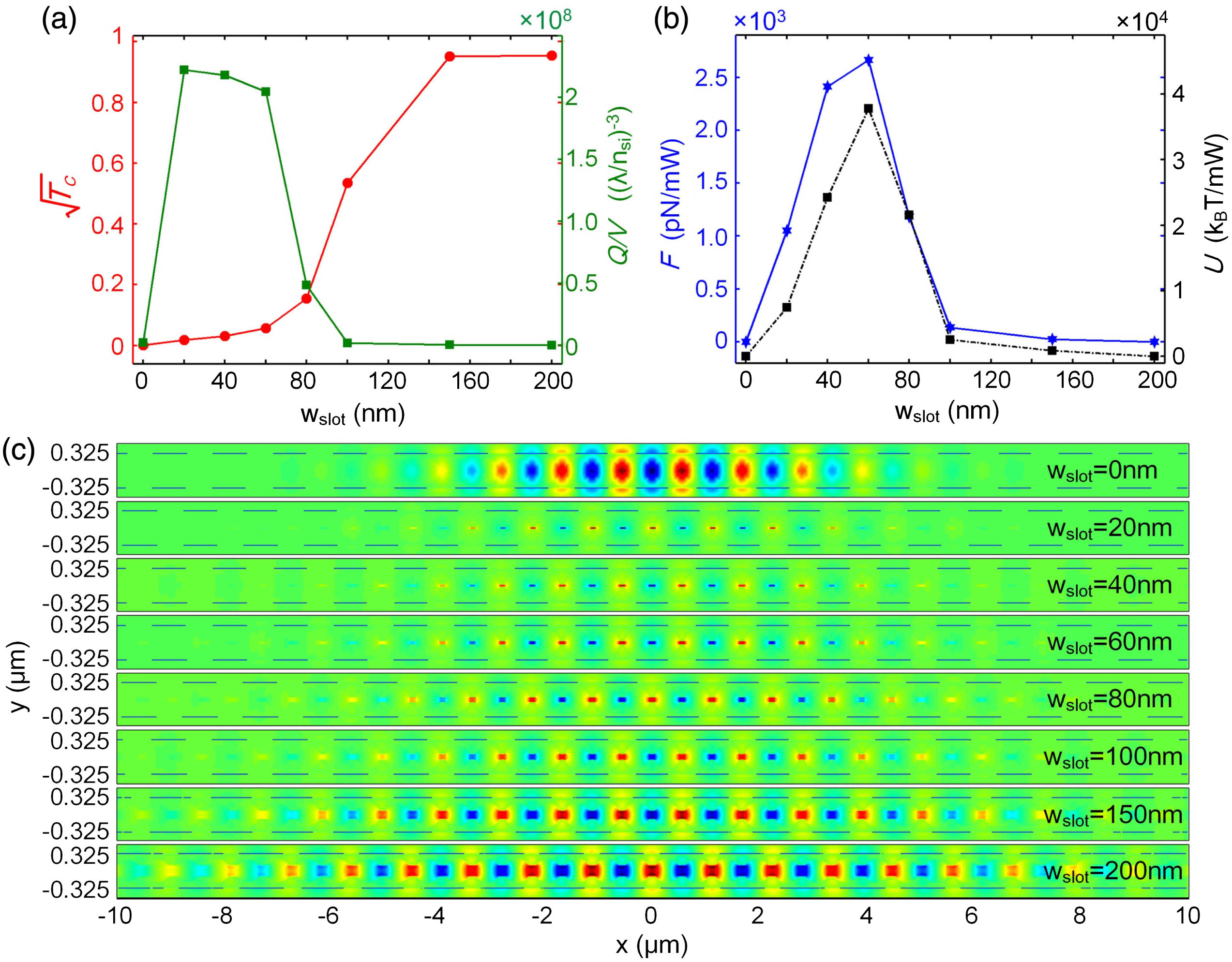
    Fig. 2. Influence of different slot widths on (a) cavity transmissivity Tc and Q/V, (b) maximum optical trapping force F and trapping potential U on a 10 nm radius PS nanoparticle, and (c) electric field Ey distributions (top view) taken at the center of the silicon layer (z=0) when wslot is changed from 0 to 200 nm and other parameters are kept fixed as wnb=650  nm, h=220  nm, a=560  nm, rcenter=0.42a, rend=0.36a, Nt=20, and Nm=10.
    Influence of different hole grating numbers Nt (changed from Nt=5 to Nt=40) in the taper region of the cavity on (a) cavity transmissivity Tc and Q/V, and (b) maximum optical trapping force F and trapping potential U on a 10 nm radius PS nanoparticle when Nm=10. Influence of different hole grating numbers Nm (changed from Nm=0 to Nm=30) in the mirror region of the cavity on (d) cavity transmissivity Tc and Q/V, and (e) maximum optical trapping force F and trapping potential U on a 10 nm radius PS nanoparticle when Nt=20. For both cases, other parameters are kept fixed as wnb=650 nm, h=220 nm, wslot=60 nm, a=560 nm, rcenter=0.42a, and rend=0.36a. (c), (f) Normalized optical trapping force F for the proposed cavity with different values of Tc·Q/V.
    Fig. 3. Influence of different hole grating numbers Nt (changed from Nt=5 to Nt=40) in the taper region of the cavity on (a) cavity transmissivity Tc and Q/V, and (b) maximum optical trapping force F and trapping potential U on a 10 nm radius PS nanoparticle when Nm=10. Influence of different hole grating numbers Nm (changed from Nm=0 to Nm=30) in the mirror region of the cavity on (d) cavity transmissivity Tc and Q/V, and (e) maximum optical trapping force F and trapping potential U on a 10 nm radius PS nanoparticle when Nt=20. For both cases, other parameters are kept fixed as wnb=650  nm, h=220  nm, wslot=60  nm, a=560  nm, rcenter=0.42a, and rend=0.36a. (c), (f) Normalized optical trapping force F for the proposed cavity with different values of Tc·Q/V.
    Numerical analysis of optical trapping forces for the proposed nanoslotted-1D-PCNC device. All theoretically computed and 3D-FEM simulated trapping forces listed are normalized by input power in units of pN/mW. Trapping force profiles of (a) Fx and (b) Fz for the PS nanoparticle as it is moved along the x-axis and z-axis of the device, respectively. In both (a) and (b), all calculations are done for a PS nanoparticle with a radius of 10 nm. Trapping potential distributions experienced by the PS nanoparticle along (c) the x-direction (ranging from x=−200 nm to x=200 nm) and (d) the z-direction (ranging from z=0 to z=200 nm).
    Fig. 4. Numerical analysis of optical trapping forces for the proposed nanoslotted-1D-PCNC device. All theoretically computed and 3D-FEM simulated trapping forces listed are normalized by input power in units of pN/mW. Trapping force profiles of (a) Fx and (b) Fz for the PS nanoparticle as it is moved along the x-axis and z-axis of the device, respectively. In both (a) and (b), all calculations are done for a PS nanoparticle with a radius of 10 nm. Trapping potential distributions experienced by the PS nanoparticle along (c) the x-direction (ranging from x=200  nm to x=200  nm) and (d) the z-direction (ranging from z=0 to z=200  nm).
    (a) 3D-FEM simulated the resonant peak wavelength of the transmission spectrum of the designed slotted 1D-PCNC when no nanoparticle is trapped and when a PS nanoparticle with a radius of 5, 10, 15, 20, or 25 nm is trapped at the cavity center with x=0, y=0, and z=0. (b) The graph shows the magnitude of the maximum trapping force Fx in the x-direction as a function of the PS nanoparticle with different sizes.
    Fig. 5. (a) 3D-FEM simulated the resonant peak wavelength of the transmission spectrum of the designed slotted 1D-PCNC when no nanoparticle is trapped and when a PS nanoparticle with a radius of 5, 10, 15, 20, or 25 nm is trapped at the cavity center with x=0, y=0, and z=0. (b) The graph shows the magnitude of the maximum trapping force Fx in the x-direction as a function of the PS nanoparticle with different sizes.
    Trapping SystemTrapping Particle Radius (nm)Trapping Force (pN/mW)Trapping Potentiala(kBT/mW)Trapping Stiffness (pN·nm1·mW1)Threshold Power (μW)References
    Solid waveguidePS, 2500.025[25]
    Slotted waveguidePS, 100.0071.41.31×1047.14×103[28]
    Ring resonatorPS, 2500.165.563.7×1041.8×103[29]
    2D-PCPS, 2503.8576.90.3130[39]
    1D-PCPS, 502.331.3320[40]
    PS, 504.2512.23×102196[41]
    PS, 100330[49]
    Slotted 2D-PCPS, 25463.77×1020.3427[53]
    Slotted 1D-PCNCPS, 108.28×1031.15×1051678.70×102Present work
    Table 1. Trapping Force, Trapping Potential, Trapping Stiffness, and Threshold Power of Various Optical Trapping Schemes
    Daquan Yang, Fei Gao, Qi-Tao Cao, Chuan Wang, Yuefeng Ji, Yun-Feng Xiao. Single nanoparticle trapping based on on-chip nanoslotted nanobeam cavities[J]. Photonics Research, 2018, 6(2): 99
    Download Citation