• Photonics Research
  • Vol. 6, Issue 2, 99 (2018)
Daquan Yang1、2、†, Fei Gao3、†, Qi-Tao Cao3, Chuan Wang2, Yuefeng Ji1、2, and Yun-Feng Xiao3、4、*
Author Affiliations
  • 1School of Information and Communication Engineering, Beijing University of Posts and Telecommunications, Beijing 100876, China
  • 2State Key Laboratory of Information Photonics and Optical Communications, Beijing University of Posts and Telecommunications, Beijing 100876, China
  • 3State Key Laboratory for Mesoscopic Physics, School of Physics, Peking University, Collaborative Innovation Center of Quantum Matter, Beijing 100871, China
  • 4Collaborative Innovation Center of Extreme Optics, Shanxi University, Taiyuan, Shanxi 030006, China
  • show less
    DOI: 10.1364/PRJ.6.000099 Cite this Article Set citation alerts
    Daquan Yang, Fei Gao, Qi-Tao Cao, Chuan Wang, Yuefeng Ji, Yun-Feng Xiao. Single nanoparticle trapping based on on-chip nanoslotted nanobeam cavities[J]. Photonics Research, 2018, 6(2): 99 Copy Citation Text show less

    Abstract

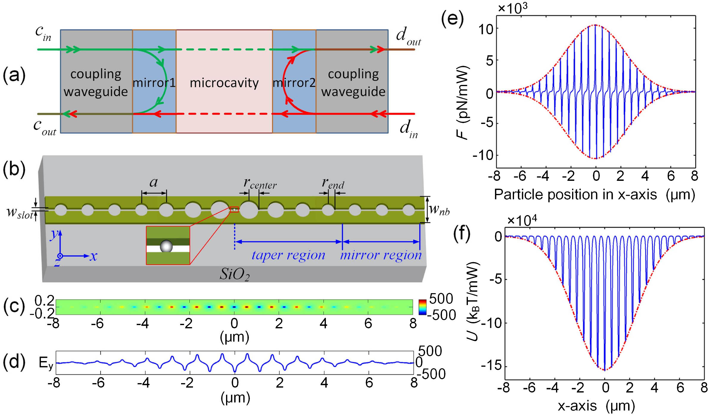
    Optical trapping techniques are of great interest since they have the advantage of enabling the direct handling of nanoparticles. Among various optical trapping systems, photonic crystal nanobeam cavities have attracted great attention for integrated on-chip trapping and manipulation. However, optical trapping with high efficiency and low input power is still a big challenge in nanobeam cavities because most of the light energy is confined within the solid dielectric region. To this end, by incorporating a nanoslotted structure into an ultracompact one-dimensional photonic crystal nanobeam cavity structure, we design a promising on-chip device with ultralarge trapping potential depth to enhance the optical trapping characteristic of the cavity. In this work, we first provide a systematic analysis of the optical trapping force for an airborne polystyrene (PS) nanoparticle trapped in a cavity model. Then, to validate the theoretical analysis, the numerical simulation proof is demonstrated in detail by using the three-dimensional finite element method. For trapping a PS nanoparticle of 10 nm radius within the air-slot, a maximum trapping force as high as 8.28 nN/mW and a depth of trapping potential as large as 1.15×10⁵ kBT mW 1 are obtained, where kB is the Boltzmann constant and T is the system temperature. We estimate a lateral trapping stiffness of 167.17 pN·nm 1· mW 1 for a 10 nm radius PS nanoparticle along the cavity x-axis, more than two orders of magnitude higher than previously demonstrated on-chip, near field traps. Moreover, the threshold power for stable trapping as low as 0.087 μW is achieved. In addition, trapping of a single 25 nm radius PS nanoparticle causes a 0.6 nm redshift in peak wavelength. Thus, the proposed cavity device can be used to detect single nanoparticle trapping by monitoring the resonant peak wavelength shift. We believe that the architecture with features of an ultracompact footprint, high integrability with optical waveguides/circuits, and efficient trapping demonstrated here will provide a promising candidate for developing a lab-on-a-chip device with versatile functionalities.
    dout=κw2adin,dadt=κs+κw2aiΔωa+κw2(cin+din),cout=κw2acin,(1)

    View in Article

    a=κw2κw+κs2+iΔωcin,cout=κs2iΔωκw+κs2+iΔωcin,dout=κw2κw+κs2+iΔωcin.(2)

    View in Article

    W=κw2(κw+κs2)2+(Δω)2Pin,R=(κs2)2+(Δω)2(κw+κs2)2+(Δω)2,Tc=(κw2)2(κw+κs2)2+(Δω)2.(3)

    View in Article

    Tc_max=κw2(κw+κs)2=Q2Qw2,Wmax=2κw(κw+κs)2Pin=2ω0QTc_maxPin.(4)

    View in Article

    F=12P·E,(5)

    View in Article

    F(r)=αW4Vc[f(r)2]=α2ω0·QTcVcPin·[f(r)2],(6)

    View in Article

    f(r)2=pE2(r)dVEmax2Vp,(7)

    View in Article

    U=αW4Vc·f(r)2=α2ω0·QTcVcPin·f(r)2.(8)

    View in Article

    kx=Fxx|x=0,y=0,z=0,(9)

    View in Article

    kz=Fzz|x=0,y=0,z=0.(10)

    View in Article

    Strap=ΔUkBT.(11)

    View in Article

    Daquan Yang, Fei Gao, Qi-Tao Cao, Chuan Wang, Yuefeng Ji, Yun-Feng Xiao. Single nanoparticle trapping based on on-chip nanoslotted nanobeam cavities[J]. Photonics Research, 2018, 6(2): 99
    Download Citation