• Journal of Semiconductors
  • Vol. 45, Issue 3, 032502 (2024)
Chao Feng1、2, Xinyue Dai1、2, Qimeng Jiang1、2、*, Sen Huang1、2、**, Jie Fan1, Xinhua Wang1、2, and Xinyu Liu1、2
Author Affiliations
  • 1Institute of Microelectronics, Chinese Academy of Sciences, Beijing 100029, China
  • 2University of Chinese Academy of Sciences, Beijing 100049, China
  • show less
    DOI: 10.1088/1674-4926/45/3/032502 Cite this Article
    Chao Feng, Xinyue Dai, Qimeng Jiang, Sen Huang, Jie Fan, Xinhua Wang, Xinyu Liu. A novel one-time-programmable memory unit based on Schottky-type p-GaN diode[J]. Journal of Semiconductors, 2024, 45(3): 032502 Copy Citation Text show less
    (Color online) Schematic diagram of the process flow of the Schottky-type p-GaN HEMT.
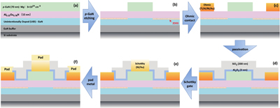
    Fig. 1. (Color online) Schematic diagram of the process flow of the Schottky-type p-GaN HEMT.
    (Color online) (a) Schematic structure of the Schottky-type p-GaN gate AlGaN/GaN HEMTs. (b) Physical image of the devices under the optical microscope. (c) Double-sweep ID−VG characteristic (black) and the IG−VG curve (blue) of the HEMT measured at a VDS of 1 V.
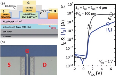
    Fig. 2. (Color online) (a) Schematic structure of the Schottky-type p-GaN gate AlGaN/GaN HEMTs. (b) Physical image of the devices under the optical microscope. (c) Double-sweep IDVG characteristic (black) and the IGVG curve (blue) of the HEMT measured at a VDS of 1 V.
    (Color online) (a) Programming process of the Schottky-type p-GaN diode-based OTP device. (b) The schematic of a 2 × 2 OTP array.
    Fig. 3. (Color online) (a) Programming process of the Schottky-type p-GaN diode-based OTP device. (b) The schematic of a 2 × 2 OTP array.
    (Color online) (a) Comparison of the anode current before and after programming (inset shows the read voltage margin). (b) Statistics of programming voltage for 60 devices.
    Fig. 4. (Color online) (a) Comparison of the anode current before and after programming (inset shows the read voltage margin). (b) Statistics of programming voltage for 60 devices.
    (Color online) (a) Program time under different program voltages (three devices each) . (b) Breakdown characteristics of the PIN junction of the p-GaN diode.
    Fig. 5. (Color online) (a) Program time under different program voltages (three devices each) . (b) Breakdown characteristics of the PIN junction of the p-GaN diode.
    (Color online) Current ratio after different read cycles at a read voltage of 3 V (a) and 6 V (b). Pulse frequency: 1 Hz to 1 MHz, pulse duty cycle: 50%.
    Fig. 6. (Color online) Current ratio after different read cycles at a read voltage of 3 V (a) and 6 V (b). Pulse frequency: 1 Hz to 1 MHz, pulse duty cycle: 50%.
    (Color online) (a) Weibull distribution of the breakdown time of the Schottky junction in the p-GaN diode. (b)Reverse bias voltages for a 10-year lifetime extracted from exponential and power laws at a 63.2% failure rate.
    Fig. 7. (Color online) (a) Weibull distribution of the breakdown time of the Schottky junction in the p-GaN diode. (b)Reverse bias voltages for a 10-year lifetime extracted from exponential and power laws at a 63.2% failure rate.
    Chao Feng, Xinyue Dai, Qimeng Jiang, Sen Huang, Jie Fan, Xinhua Wang, Xinyu Liu. A novel one-time-programmable memory unit based on Schottky-type p-GaN diode[J]. Journal of Semiconductors, 2024, 45(3): 032502
    Download Citation