Abstract
In this work, a novel one-time-programmable memory unit based on a Schottky-type p-GaN diode is proposed. During the programming process, the junction switches from a high-resistance state to a low-resistance state through Schottky junction breakdown, and the state is permanently preserved. The memory unit features a current ratio of more than 103, a read voltage window of 6 V, a programming time of less than 10?4 s, a stability of more than 108 read cycles, and a lifetime of far more than 10 years. Besides, the fabrication of the device is fully compatible with commercial Si-based GaN process platforms, which is of great significance for the realization of low-cost read-only memory in all-GaN integration.Introduction
Gallium nitride (GaN)-based devices have gained considerable recognition in the field of power electronics, owing to their remarkable attributes such as high electron mobility, high electron saturation drift velocity, and high breakdown electric field[1, 2]. Presently, commercial silicon-based GaN platforms have successfully integrated various electrical components like capacitors, resistors, diodes, and enhancement/depletion (E/D) mode high electron mobility transistors (HEMTs)[3, 4]. However, research on on-chip memory devices remains limited, which is crucial for improving the performance, power efficiency, security, and reliability of all-GaN integrated circuits. It has been reported that some non-volatile memory (NVM) cells use the fast-trap/slowly-detrap of carriers as program/erase behavior of the information[5, 6], some resistive random access memory (RRAM) devices use the switching of high/low resistance state (HRS/LRS) after soft breakdown as a set/reset process[7]. Additionally, static random-access memory (SRAM) arrays have been achieved through the integration of highly uniform E/D mode GaN devices[8]. However, these technologies are either difficult to compatible with the existing GaN process, or are too complex and cost-prohibitive, which limits their large-scale application. The anti-fuse one-time-programmable (OTP) memory device, emerges as a cost-effective read-only memory (ROM), making it an invaluable component in applications emphasizing data security, firmware or configuration storage, and resistance to tampering.
Fortunately, the circuit model of the Schottky-type p-GaN diode (metal/p-GaN/AlGaN/GaN stack)[9], is very similar to the diode-based OTP unit in Si complementary metal-oxide semiconductor (CMOS) technology[10−12]. Thus, for the first time, a p-GaN diode-based anti-fuse OTP device that switches from HRS to LRS by controlling Schottky junction breakdown, is presented in this letter. Besides, p-GaN diode-based OTP devices are fully compatible with commercial p-GaN processes and can achieve high integration at low cost. Furthermore, the unique properties of p-GaN diodes, including their inherent stability, high thermal conductivity, and resistance to harsh environmental conditions, make them an intriguing candidate for OTP memory technology[13].
Device fabrication and operation mechanism
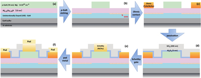
In this study, the p-GaN heterostructure is deposited on a 6-inch Si substrate, comprising a GaN buffer layer, a 200 nm unintentionally doped (UID) GaN layer, a 15 nm Al0.22Ga0.78N barrier layer, and a 70 nm p-GaN layer with Mg doping concentration of 3 × 1019 cm−3. The fabrication of the Schottky-type p-GaN gate HEMTs aligns with our previous work[14], as shown in Fig. 1, starting with the formation of the p-GaN gate by two-step etching process (a rapid Cl2/BCl3-based inductively coupled plasma-etching and a high-selectivity, low-damage self-stopping ICP etching based on Cl2/N2/O2), followed by Ti/Al/Ni/Au (20/150/55/45 nm) source/drain Ohmic contacts evaporation. The passivation layer consists of 3 nm atomic layer deposition (ALD)-Al2O3 and 200 nm plasma-enhanced chemical vapor deposition (PECVD)-SiO2. The schematic and the physical image of the fabricated HEMT is depicted in Figs. 2(a) and 2(b), respectively. Devices feature a gate length/width (LG/WG) of 4/100 μm and a gate-source/drain separation (LGS/LGD) of 4/4 μm. Fig. 2(c) shows the double-sweep ID−VG characteristic and the IG−VG curve of the HEMT measured at a VDS of 1 V, the device exhibits a threshold voltage (VTH) of approximately 1 V, confirming the normal electrical characteristics.

Figure 1.(Color online) Schematic diagram of the process flow of the Schottky-type p-GaN HEMT.
Figure 2.(Color online) (a) Schematic structure of the Schottky-type p-GaN gate AlGaN/GaN HEMTs. (b) Physical image of the devices under the optical microscope. (c) Double-sweep ID−VG characteristic (black) and the IG−VG curve (blue) of the HEMT measured at a VDS of 1 V.
The gate region of the Schottky-type p-GaN gate HEMT can be equivalently represented as a series of a Schottky barrier diode (SBD) and a PIN diode[9], as illustrated in Fig. 3(a). When the source and drain of the HEMT are shorted, the gate and 2DEG channel can be regarded as the anode and cathode of a diode, respectively (this study aims to verify the feasibility of p-GaN diodes in OTP arrays, and the junction area is approximately 400 μm²; for practical OTP arrays, reducing the junction area is required to achieve high integration). When a large programming voltage (Vprogram) is applied to the anode, the capacitive voltage divider relationship determines that most of the voltage drops on the Schottky junction, leading to its degradation until catastrophic breakdown[15, 16]. At this point, the Schottky junction loses its rectification ability, transitioning from HRS to LRS, and becomes irrecoverable. This naturally forms an anti-fuse structure in the p-GaN system.
Figure 3.(Color online) (a) Programming process of the Schottky-type p-GaN diode-based OTP device. (b) The schematic of a 2 × 2 OTP array.
Performance of the OTP memory
To achieve integration, multiple diodes can be connected with the anodes to the word lines (WL) and the cathodes to the bit lines (BL) to create an OTP storage array. Fig. 3(b) displays the schematic of a simplified 2 × 2 OTP array. During the programming of Unit 2, WL2 is pulled up to the Vprogram, while BL1 is grounded. A voltage of Vprogram−VPIN drops on the Schottky junction, causing the degradation, where VPIN is the forward turn-on voltage of the PIN junction. For read operations, a relatively small read voltage (Vread) is applied to WL2. The current through unprogrammed devices is small due to the reverse bias of the Schottky junction, while programmed devices exhibit a significant current as the PIN junction is turned on. Fig. 4(a) shows a comparison of the anode current before and after programming of the p-GaN diode-based OTP device. It is observed that the current ratio (IA_programmed/IA_unprogrammed) reaches up to 103 at Vread = 3 V, and the Vread window is approximately 6 V when the current ratio is larger than 102 (inset of Fig. 4(a)), which indicates that the OTP device provides a sufficient margin to avoid faulty reading. It is worth noting that selecting appropriate high work-function anode metals can increase the Schottky barrier, further reducing the current in unprogrammed devices and increasing the current ratio[17]. The programming voltage distribution of 60 OTP units is shown in Fig. 4(b), revealing a standard deviation of only 0.8 V, demonstrating strict control over programming conditions.
Figure 4.(Color online) (a) Comparison of the anode current before and after programming (inset shows the read voltage margin). (b) Statistics of programming voltage for 60 devices.
In practical applications, Vprogram is often applied to OTP devices in the form of pulses, therefore, it requires the programming time (tprogram) to align with the clock frequency of the circuit. Fig. 5(a) shows the temporal characteristics of the anode current at different programming voltages. As the Vprogram increases from 7.5 to 9 V, the tprogram decreases from 102 to 10−2 s. Increasing the programming voltage can further reduce the programming time (when Vprogram is 9.2 V, the tprogram is less than the device sampling resolution of 10−4 s).
Figure 5.(Color online) (a) Program time under different program voltages (three devices each) . (b) Breakdown characteristics of the PIN junction of the p-GaN diode.
During programming operations on Unit 2, BL2 is raised to Vprogram simultaneously with WL2, while WL1 is grounded along with BL1 to prevent accidental programming of Unit 4 and Unit 1. In this case, Unit 3 requires a strong ability to withstand high reverse bias voltage. Fig. 5(b) illustrates the reverse breakdown characteristics of the PIN junction of the p-GaN diode. Even when the reverse bias voltage is increased to 100 V, the leakage current remains at the level of 10−9 A, indicating its reverse voltage blocking ability.
When performing read operations on programmed devices, the PIN junction is in a forward-biased state. Although a small read voltage could hardly induce any degradation of the PIN junction, we still evaluated the device's reliability during read operations, which is akin to retention time. Here, AC pulse signals of 3 and 6 V (pulse duty cycle of 50 %) are applied to the anode of the OTP device to simulate read pulses, respectively. After undergoing varying numbers of read cycles, the current ratio is extracted, as shown in Fig. 6. At different pulse frequencies (from 1 Hz to 1 MHz), the pulse count is adjusted (from 102 to 108) to ensure the same effective read time of 50 s. The results indicate that even after 108 read cycles at Vread = 6 V, the current ratio of p-GaN diode-based OTP devices remains unchanged, demonstrating its stability during prolonged read operations.
Figure 6.(Color online) Current ratio after different read cycles at a read voltage of 3 V (a) and 6 V (b). Pulse frequency: 1 Hz to 1 MHz, pulse duty cycle: 50%.
During the reading operations of Unit 2, a small read voltage (about 3 V) is applied to WL2 as well. Though the Vread is much lower than the Vprogram, the Schottky junction of Unit 4 would remain in the reverse bias, posing a risk of unintended programming. Fig. 7(a) demonstrates that the breakdown time of the Schottky junction in the p-GaN diode follows a Weibull distribution, consistent with widely reported gate failure in p-GaN HEMTs[18−20]. At different reverse bias voltages, the shape parameter (β) of the Weibull distribution almost exceeds 1, indicating a significant reduction in externally triggered breakdown mechanisms associated with defects[15]. From exponential and power laws at a 63.2% failure rate, reverse bias voltages for a 10-year lifetime are estimated to be 4.9 and 5.6 V, respectively, as shown in Fig. 7(b). This ensures the reliability of the p-GaN diode-based OTP devices when operating at 3 V read voltage for a longer operation time.
Figure 7.(Color online) (a) Weibull distribution of the breakdown time of the Schottky junction in the p-GaN diode. (b)Reverse bias voltages for a 10-year lifetime extracted from exponential and power laws at a 63.2% failure rate.
Conclusion
In this work, a promising p-GaN diode-based OTP memory device for GaN-based power electronics is proposed. The performance of the OTP device covers a current ratio of more than 103, a read voltage window of 6 V, a programming time of less than 10−4 s, a strong reverse voltage blocking ability, a stability of more than 108 read cycles and a lifetime of over 10 years. Further works, such as improving noise margin, device scaling-down, and integration, are worth carrying out.
References
[1] K J Chen, O Häberlen, A Lidow et al. GaN-on-Si power technology: Devices and applications. IEEE Trans Electron Devices, 64, 779(2017).
[2] H Amano, Y Baines, M Borga et al. The 2018 GaN power electronics roadmap. J Phys D: Appl Phys, 51, 163001.
[3] Z Y Zheng, L Zhang, W J Song et al. Gallium nitride-based complementary logic integrated circuits. Nat Electron, 4, 595(2021).
[4] Z Zheng, H Xu, L Zhang et al. On the operating speed and energy efficiency of GaN-based monolithic complementary logic circuits for integrated power conversion systems. Fundamental Research, 661.
[5] Y R Chen, H Song, H Jiang et al. Reproducible bipolar resistive switching in entire nitride AlN/n-GaN metal-insulator-semiconductor device and its mechanism. Appl Phys Lett, 105, 193502(2014).
[6] T Chen, Z Y Zheng, S R Feng et al. Endurance improvement of GaN bipolar charge trapping memory with back gate injection. IEEE Electron Device Lett, 44, 1408(2023).
[7] K Fu, H Q Fu, X Q Huang et al. Threshold switching and memory behaviors of epitaxially regrown GaN-on-GaN vertical p-n diodes with high temperature stability. IEEE Electron Device Lett, 40, 375(2019).
[8] M Y Yuan, Q Y Xie, J Niroula et al. GaN memory operational at 300 °C. IEEE Electron Device Lett, 43, 2053(2022).
[9] L Sayadi, G Iannaccone, S Sicre et al. Threshold voltage instability in p-GaN gate AlGaN/GaN HFETs. IEEE Trans Electron Devices, 65, 2454(2018).
[10] J He, W T Chan, C Wang et al. A compact CMOS compatible oxide antifuse with polysilicon diode driver. IEEE Trans Electron Devices, 59, 2539(2012).
[11] R J Kuo, F C Chang, Y C King et al. Antifuse OTP cell in a cross-point array by advanced CMOS FinFET process. IEEE Trans Electron Devices, 66, 1729(2019).
[12] K P Ng, M C Lee, K C Kwong et al. Diode based gate oxide anti-fuse one time programmable memory array in standard CMOS process, 457(2010).
[13] B N Pushpakaran, A S Subburaj, S B Bayne. Commercial GaN-based power electronic systems: A review. J Electron Mater, 49, 6247(2020).
[14] X Y Dai, Z C Ji, Q M Jiang et al. Suppression of reverse leakage in enhancement-mode GaN high-electron-mobility transistor by extended PGaN technology. Phys Status Solidi A, 220, 2200692(2023).
[15] A N Tallarico, S Stoffels, P Magnone et al. Investigation of the p-GaN gate breakdown in forward-biased GaN-based power HEMTs. IEEE Electron Device Lett, 38, 99(2017).
[16] C Feng, Q M Jiang, S Huang et al. Gate-bias-accelerated VTH recovery on schottky-type p-GaN gate AlGaN/GaN HEMTs. IEEE Trans Electron Devices, 70, 4591(2023).
[17] F Lee, L Y Su, C H Wang et al. Impact of gate metal on the performance of p-GaN/AlGaN/GaN high electron mobility transistors. IEEE Electron Device Lett, 36, 232(2015).
[18] T L Wu, D Marcon, S Z You et al. Forward bias gate breakdown mechanism in enhancement-mode p-GaN gate AlGaN/GaN high-electron mobility transistors. IEEE Electron Device Lett, 36, 1001(2015).
[19] S Stoffels, B Bakeroot, T L Wu et al. Failure mode for p-GaN gates under forward gate stress with varying Mg concentration, 4B(2017).
[20] F Masin, M Meneghini, E Canato et al. Positive temperature dependence of time-dependent breakdown of GaN-on-Si E-mode HEMTs under positive gate stress. Appl Phys Lett, 115, 052103(2019).