
Gang Xia, Wei Fan, Dajie Huang, He Cheng, Jiangtao Guo, Xiaoqin Wang. High damage threshold liquid crystal binary mask for laser beam shaping[J]. High Power Laser Science and Engineering, 2019, 7(1): 010000e9
- High Power Laser Science and Engineering
- Vol. 7, Issue 1, 010000e9 (2019)
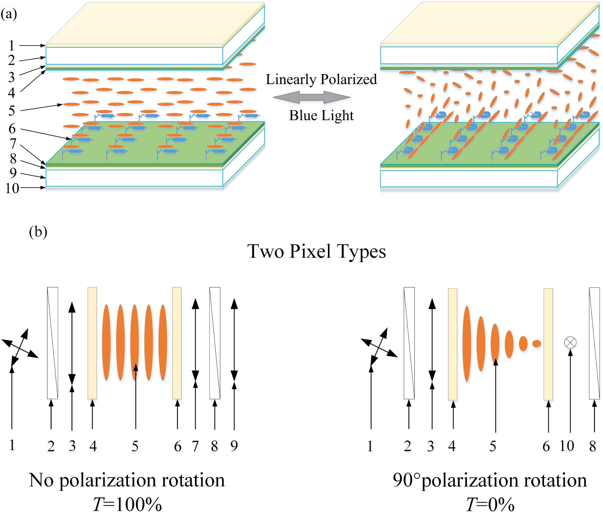
Fig. 1. (a) Structure of the LC binary mask (1 – anti-reflection coating, 2 – front glass substrate, 3 – anti-reflection coating, 4 – polyimide layer, 5 – LC molecule, 6 – azobenzene group, 7 – photoalignment layer, 8 – anti-reflection coating, 9 – rear glass substrate and 10 – anti-reflection coating) and (b) arrangement of LC molecules in a single pixel of two pixel types (1 – incident light, 2 – polarizer, 3 – P-polarized light, 4 – front glass substrate with coating polyimide, 5 – LC molecule, 6 – rear glass substrate with coating azobenzene, 7 – P-polarized light, 8 – polarizer, 9 – output light and 10 – S-polarized light).
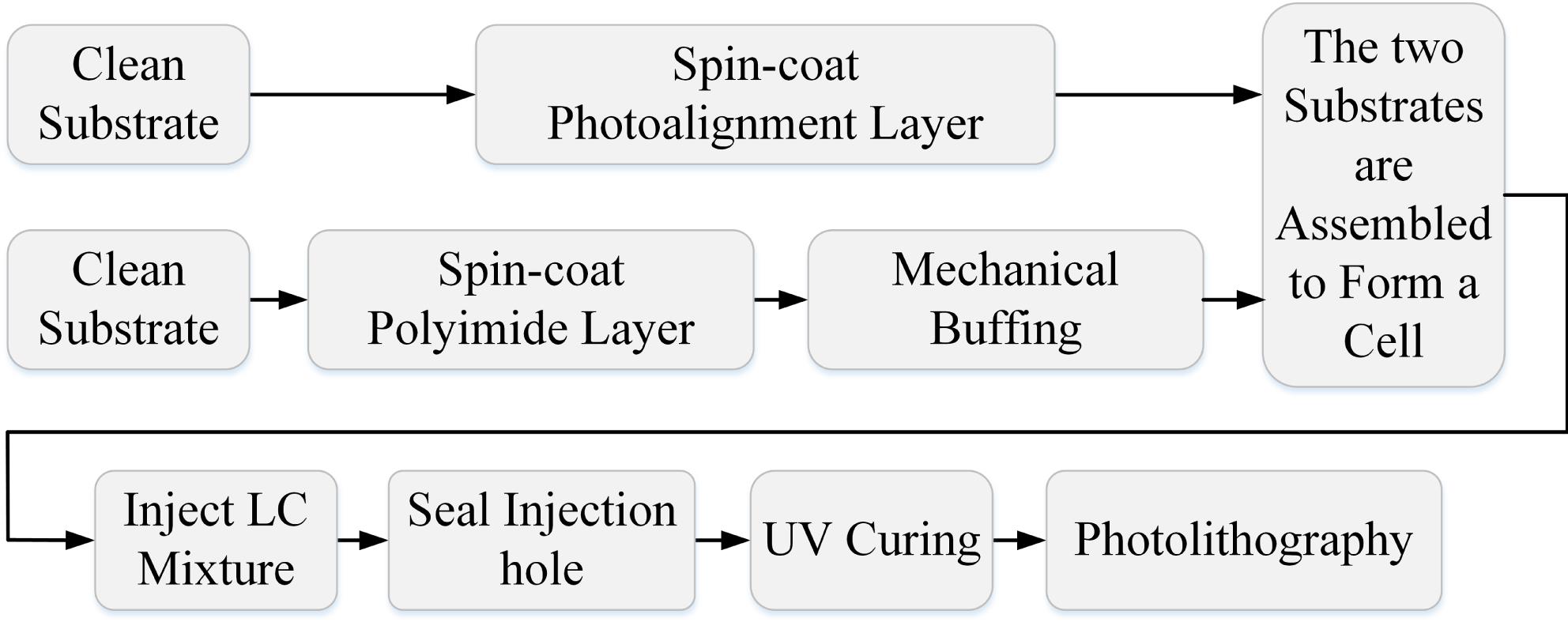
Fig. 2. Fabrication process of the LC cell.
Fig. 3. Photolithography mask system (1 – light source, 2 – collimating lens, 3 – polarization beam splitter, 4 – LCOS, 5 – imaging system (1:1) and 6 – LC cell).
Fig. 4. Designed objective function $y=0.8x^{2}+0.2$ . (a) Binary distribution of the mask; the unit pixel is $40~\unicode[STIX]{x03BC}\text{m}$ . (b) Spatial distribution of the objective function.
Fig. 5. Beam shaping test system (1 – laser source, 2 – single mode fiber, 3 – fiber port, 4 – beam expander ($20\times$ ), 5 – polarization beam splitter, 6 – LC binary mask, 7 – polarization beam splitter, 8 – plano-convex lens, 9 – mirror, 10 – pinhole, 11 – mirror, 12 – plano-convex lens and 13 – CCD).
Fig. 6. Physical LC binary mask. (a) Boundary dimension of the physical LC binary mask. (b) Parabolic pixel distribution is observed in polarized white light. (c) Regional area of the pixel structure examined under a crossed polarizer microscope ($50\times$ ).
Fig. 7. Parabolic shaping of the LC binary mask (curve 1 is the designed objective function, curve 2 was tested at the completed mask; curve 3 is the transmission curve of the same tested mask, which has been stored for six months in a conventional storage).
Fig. 8. Square soft edge diaphragm of the LC binary mask.
Fig. 9. Logo picture of ‘SIOM’ (the size of the picture is 8 mm $\times$ 8 mm; (a) designed picture and (b) picture written on the LC cell).
Fig. 10. Results of written and erased situation. (a) First lithography. (b) Third lithography on the same LC cell. (c) Fifth lithography on the same LC cell. (d) Sixth lithography on the same LC cell. (e) The LC cell erased by a linearly polarized blue light of 10 mW for 5 minutes after the sixth writing. (f) The LC cell erased at the power of 10 mW for extra 3 hours after (e).
|
Table 1. Laser damage thresholds of the azobenzene-based photoalignment layers.
|
Table 2. Laser damage thresholds of the LC binary mask materials.

Set citation alerts for the article
Please enter your email address
© Copyright 2018-2021 | Chinese Laser Press. All Rights Reserved 沪ICP备15018463号-20