• High Power Laser Science and Engineering
  • Vol. 7, Issue 1, 010000e9 (2019)
Gang Xia1、2、3, Wei Fan1、2, Dajie Huang1、2, He Cheng1、2, Jiangtao Guo1、2、3, and Xiaoqin Wang1、2、3
Author Affiliations
  • 1Key Laboratory of High Power Laser and Physics, Shanghai Institute of Optics and Fine Mechanics, Chinese Academy of Sciences, Shanghai 201800, China
  • 2National Laboratory on High Power Laser and Physics, Shanghai Institute of Optics and Fine Mechanics, Chinese Academy of Sciences, Shanghai 201800, China
  • 3University of Chinese Academy of Sciences, Beijing 100049, China
  • show less
    DOI: 10.1017/hpl.2018.69 Cite this Article Set citation alerts
    Gang Xia, Wei Fan, Dajie Huang, He Cheng, Jiangtao Guo, Xiaoqin Wang. High damage threshold liquid crystal binary mask for laser beam shaping[J]. High Power Laser Science and Engineering, 2019, 7(1): 010000e9 Copy Citation Text show less

    Abstract

    In order to improve the damage threshold and enlarge the aperture of a laser beam shaper, photolithographic patterning technology is adopted to design a new type of liquid crystal binary mask. The inherent conductive metal layer of commercial liquid crystal electro-optical spatial light modulators is replaced by azobenzene-based photoalignment layers patterned by noncontact photolithography. Using the azobenzene-based photoalignment layer, a liquid crystal binary mask for beam shaping is fabricated. In addition, the shaping ability, damage threshold, write/erase flexibility and stability of the liquid crystal binary mask are tested. Using a 1 Hz near-IR (1064 nm) laser, the multiple-shot nanosecond damage threshold of the liquid crystal mask is measured to be higher than $15~\text{J}/\text{cm}^{2}$. The damage threshold of the azobenzene-based photoalignment layer is higher than $50~\text{J}/\text{cm}^{2}$ under the same testing conditions.

    1 Introduction

    In a high-power and high-energy laser system, the injected laser beam needs to be shaped for a special geometric outline and spatial intensity distribution[1]. Dielectric binary masks have high damage threshold, but the production cycle is long, and the largest aperture can be 50 mm $\times$ 50  mm[2]. Owing to the cost-effectiveness and flexibility of liquid crystal (LC) optical elements for laser beam shaping, commercial electrically or optically addressed LC spatial light modulators and chrome binary masks are most widely used in the near-field beam shaping; however, their laser damage threshold is $130~\text{mJ}/\text{cm}^{2}$ (1053 nm, 3 ns, 1 Hz)[36]. Because of their inherent conductive metal layer (such as indium tin oxide, ITO), they can only be applied to low-fluence areas of the laser power. Recently, a high damage threshold LC laser beam shaper has been developed at the University of Rochester’s Laboratory for Laser Energetics (LLE); they used cinnamate or coumarin photoalignment layers to replace the metal layer of a commercial LC spatial light modulator and achieve the alignment of LC molecules on a glass substrate[26]. The shaping pattern can be written in the LC cell. Furthermore, the laser damage threshold of cinnamate and coumarin photoalignment layers can reach that of bare fused silica ($30{-}60~\text{J}/\text{cm}^{2}$, 1054 nm, 1 ns, 1 Hz), but the shaping pattern cannot be changed once it has been written[4].

    Flexibility is in demand for high power laser beam shapers. Electrically or optically addressed LC on a silicon spatial light modulator (LCOS-SLM) can realize real-time adjustment for laser beam shaping[710]. Thus, the LLE tested several commercial azobenzene-based photoswitchable alignment materials in 2013, as azobenzene materials can align LC molecules flexibly[8]. They are coated on substrates to reorient LC molecules by means of reversible optical switching between two predetermined alignment patterns, using low-energy polarized ultraviolet (UV)/visible incident light. However, the disadvantage of azobenzene materials is short-term stability of these material coatings. When the coatings are exposed to an LC, the LC can dissolve them thus decreasing the LC anchoring energy and reducing the contrast and lifetime of the device[11].

    In order to enlarge the aperture and improve the damage threshold and stability of the LC beam shaper, we adopted the photolithographic patterning technology based on a silicon-based LC light modulator to design a new type of binary mask as described in Refs [11, 12]. An azobenzene-based photoalignment layer was used to reorient LC molecules. Flexible and stable LC binary masks for laser beam shaping were fabricated and tested. Using a 1 Hz near-IR (1064 nm) laser, the multiple-shot nanosecond damage threshold was measured to be higher than $15~\text{J}/\text{cm}^{2}$ under the N-on-1 testing condition. The aperture was 30 mm $\times$ 30 mm, and the laser damage threshold of the azobenzene-based photoalignment layer was higher than $54~\text{J}/\text{cm}^{2}$ under the same testing conditions.

    2 Working principle

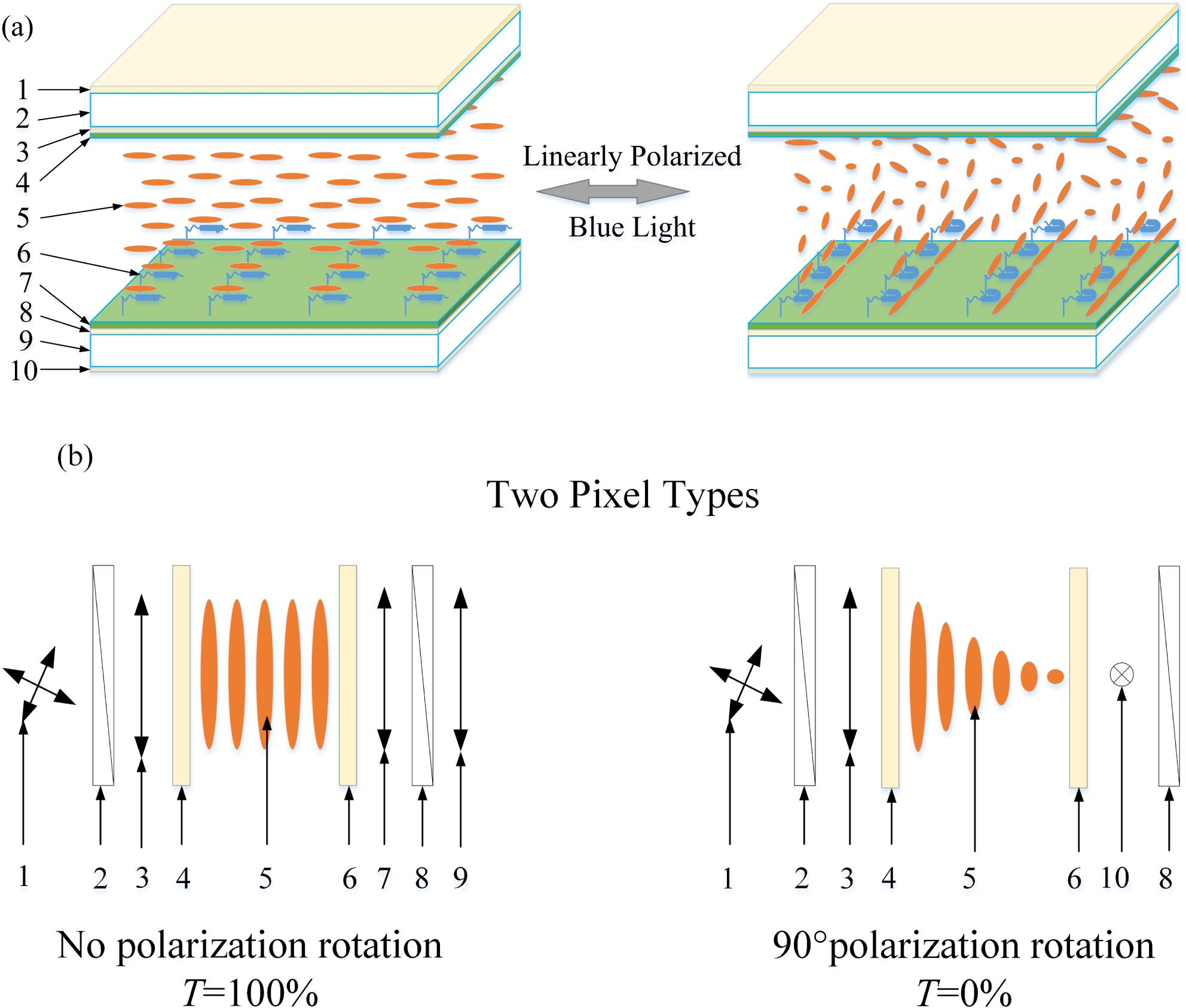
    High damage threshold laser beam shapers are based on the preparative technology of electrically addressed LC spatial light modulators. The inherent conductive metal oxide layers are replaced by commercial azobenzene-based photoalignment materials. Azobenzene-based photoalignment materials are spun to align LC molecule layers and patterned by noncontact photolithography, with a high damage threshold. An LCOS-SLM produces a low-energy linearly polarized blue-light shaping pattern, which is designed directly by using an error-diffusion algorithm and then projected on the azobenzene-based photoalignment layer of an LC binary mask. Afterward, the photoalignment layers absorb the energy of irradiated linearly polarized blue light in a given direction to keep the orientation of LC molecules, as shown in Figure 1(a). In this way, the LC binary mask can be written/erased flexibly. The orientation of LC molecules is perpendicular to the given polarization direction of an irradiated linearly polarized arbitrary shaping pattern, and the arbitrary shaping pattern is written on the LC cell at a blue-light (450 $\pm$ 9 nm) power of 10 mW, after 5 minutes.

    The LC binary mask is composed of a binary array of pixels, where the orientation of LC molecules is parallel or twisted nematic, depending on the alignment direction photopatterned on the two bounding pixel surfaces[11, 12]. Figure 1(b) is the arrangement of LC molecules on the two bounding surfaces in a single pixel. The orientation of LC molecules on the front glass substrate induced by the polyimide is parallel to the direction of a polarizer. After light is incident on the polarizer, the polarized light propagates forward along the LC molecules. The orientation of the LC molecules on the rear substrate coated with the azobenzene-based photoalignment material is determined by the polarization direction of the irradiated linearly polarized blue light. If the orientation of LC molecules on the rear substrate is parallel to the polarizer, the transmission is 100%; otherwise, the transmission is 0. The shaping function of the entire mask can be acquired accurately by controlling the transmission (0 or 100%) distribution of each pixel. When a uniform-input-polarization state is incident on the mask, it is transformed into a pixelated array of two output-polarization states that are converted into two binary transmission states after passing through the polarizer[4]. Far-field Fourier filtering of the binary output illumination results in a continuous spatial modulation of the laser beam that ‘shapes’ its intensity output[4].

    3 Experiment

    3.1 Liquid crystal cell fabrication

    The fabrication process of the LC beam shaper is shown in Figure 2. The size of K9 glass substrates is 30 mm $\times$ 30 mm $\times$ 1 mm. They are cleaned by the following steps: (1) cleaning with the neutral detergent in deionized water at $60\,^{\circ }\text{C}$ for 45 minutes by an ultrasonic cleaner, then cooling them to $20\,^{\circ }\text{C}$; (2) rinsing in the mixture of alcohol and acetone (volume ratio is 1:1); (3) scrubbing with a soft synthetic wiper to remove the residues of alcohol and acetone. Then, the substrates are subjected to ultrasonic cleaning with deionized water at $25\,^{\circ }\text{C}$ for 60 minutes, followed by drying under the electric heater at a temperature of $120\,^{\circ }\text{C}$ for 60 minutes. After the hot substrates are cooled to room temperature (${\sim}20\,^{\circ }\text{C}$), the azobenzene-based photoalignment material (PAAD-72, from Beamco, USA) is spin-deposited at 2000 r/min for 30 seconds, followed by drying for 30 seconds on a heating table at $80\,^{\circ }\text{C}$. The second cleaned glass substrate is spin-coated with polyimide (JC-TN-01-4.0%, from King Optronics Co., Ltd., China) at 3000 r/min for 20 seconds, followed by rubbing alignment after drying. Then, the two substrates are assembled to form a cell. The thickness of the cell is controlled by silica spheres dispersed in UV-curing epoxy. The diameter of the silica spheres is $4.5\pm 0.3~\unicode[STIX]{x03BC}\text{m}$, which is chosen to optimize the contrast of the mask at 1053 nm. The thickness of the LC cell is designed by the following formula, $$\begin{eqnarray}\displaystyle d=\frac{\unicode[STIX]{x1D706}\sqrt{(2n)^{2}-1}}{2\unicode[STIX]{x0394}n},n=1,2,3,\ldots . & & \displaystyle\end{eqnarray}$$ 

    After the empty LC cell is prepared, we inject the nematic LC (HPC850600, from PhiChem, China, birefringence of 0.219 at 1053 nm) and dope 0.07 wt.% chiral agent (S811, from PhiChem, China) into it by capillary action in vacuum at room temperature. For a specific incident intensity distribution, photolithography is performed by using an electrically/optically addressed LCOS-SLM for 5 minutes at a blue-light power of 10 mW[1315]. All operations above must be performed in an ultraclean room (Class 100).

    3.2 Photolithography system

    The photolithography system, shown in Figure 3 is based on a commercial electrically addressed LCOS-SLM (HOLOEYE, 1920 pixels $\times$ 1080 pixels). The blue-light source (wavelength: 420 $\pm$ 25 nm) consists of an LED and micro-lens arrays, which output a uniform beam. A parallel beam with uniform linear polarization passes through a collimating lens and a polarization beam splitter, and is modulated by the LCOS-SLM by loading the binary shaping pattern. The binary shaping pattern is a binary distribution, which is designed by an error-diffusion algorithm using the MATLAB software. The LC cell is put at the image plane of the imaging system. In photolithography, linearly polarized blue light is directly imaged on the azobenzene-based photoalignment layer through the rear glass substrate without penetrating through the LC layer. First, we set a ‘white’ pattern for the entire LC cell aperture by driving the LCOS-SLM (which is connected and controlled by a computer) to be fully transmissive. The functional group direction of the azobenzene-based photoalignment layer is perpendicular to the linearly polarized light of the LCOS-SLM output beam, which can orient LC molecules parallel to them. Second, the LC cell is rotated by $90^{\circ }$, and then we choose a designed parabolic objective function $y=0.8x^{2}+0.2$ to irradiate it; the unit pixel size is $40~\unicode[STIX]{x03BC}\text{m}$, which is shown in Figure 4. If the objective function needs to be changed, we also could set a ‘white’ pattern on the LCOS-SLM to ‘erase’ the LC mask and ‘write’ another pattern. Therefore, the LC binary mask can be written and erased flexibly.

    4 Shaping ability test system

    In order to test the shaping ability of the LC binary mask, we constructed a test system, as shown in Figure 5. The laser source can output an adjustable continuous laser beam with a maximum power of 10 mW at 1053 nm, which is injected into the $20\times$ beam expander by a single mode fiber. Two polarization beam splitters sandwich the LC binary mask, which is imaged by a telescope onto a CCD camera (the size is 1080 pixels $\times$ 768 pixels, $13.3~\unicode[STIX]{x03BC}\text{m}$). The spatial filter is a tunable pinhole inside the image relay, which can filter the high-frequency intensity modulation at appropriate diffraction limit multiples[16, 17]. We also can write or erase the LC binary mask with different patterns flexibly to test the shaping ability of the system.

    5 Experimental results and discussion

    Using the method above, the physical parabolic LC binary mask is manufactured, which is shown in Figure 6. The size of the LC binary mask is 30 mm $\times$ 30 mm, and the unit pixel is $40~\unicode[STIX]{x03BC}\text{m}\times 40~\unicode[STIX]{x03BC}\text{m}$, which is as designed. Under parallel polarizers, the parallel-aligned and twisted nematic pixels of LC molecules on two substrates appear bright and dark, respectively[18, 19]. Namely, when the functional group direction of the azobenzene-based photoalignment layer is parallel to the rubbing alignment of polyimide, the pixel is bright; otherwise, it is dark. The pixels distribution of the parabolic function can be observed in polarized white light, whose size and characteristics are the same as the designed ones. The size of a unit pixel examined under a microscope (50X) is $40~\unicode[STIX]{x03BC}\text{m}\times 40~\unicode[STIX]{x03BC}\text{m}$.

    As the laser damage threshold of electro-optical LC shaping devices depends mainly on the inherent conductive metal oxide, which is replaced by the azobenzene-based photoalignment layer, the layer laser damage threshold is tested by using a 1 Hz near-IR (1064 nm) laser. Azobenzene material is coated on two types of glass substrate (K9 and ultraclear float glass), and both are irradiated with a multiple-shot nanosecond laser (1 Hz, 1064 nm). Laser damage thresholds for N-on-1 testing the azobenzene-based photoalignment layer spun on different glass substrates are shown in Table 1. The laser damage threshold of the azobenzene material is higher than that of the chrome-plated binary mask and conductive metal oxide; it can reach $62~\text{J}/\text{cm}^{2}$. In addition, the laser damage thresholds of LC, polyimide, chemical and inorganic anti-reflection films, and glass substrate are tested and presented in Table 2. From Tables 1 and 2, the laser damage threshold of the LC binary mask mainly depends on polyimide and LC; the azobenzene-based photoalignment layer can replace the conductive metal oxide to enhance the LC binary mask damage resistance greatly.

    SubstrateLaser damage threshold@1064 nm, 10 ns, 1 Hz
    K9 glass 1$62.5385~\text{J}/\text{cm}^{2}$
    K9 glass 2$62.9698~\text{J}/\text{cm}^{2}$
    Ultraclear float glass$54.34~\text{J}/\text{cm}^{2}$

    Table 1. Laser damage thresholds of the azobenzene-based photoalignment layers.

    MaterialLaser damage
    threshold@1064 nm, 10 ns, 1 Hz
    LC ($d\sim 5~\unicode[STIX]{x03BC}\text{m}$)$18~\text{J}/\text{cm}^{2}$
    Polyimide ($d=50~\text{nm}$)$15~\text{J}/\text{cm}^{2}$
    Chemical anti-reflection film$30~\text{J}/\text{cm}^{2}$
    Inorganic anti-reflection film$15~\text{J}/\text{cm}^{2}$
    Glass substrate (K9)$50~\text{J}/\text{cm}^{2}$

    Table 2. Laser damage thresholds of the LC binary mask materials.

    The laser beam shaping ability is the key parameter to judge the performance of the LC binary mask. The transmission of the LC binary mask is the parabolic function $y=0.8x^{2}+0.2$ with an opening width of 10 mm, which is tested by using the above-mentioned shaping ability test system (Figure 5). Curve 1 is the designed transmission curve, and curve 2 is the transmission curve of the same LC binary mask tested six months ago. Curve 3 is the transmission curve of the LC binary mask, which has been stored for six months in the lab environment. The comparison of the three transmission curves is shown in Figure 7. Tested transmission curve 2 and curve 3 are in accordance with theoretically designed curve 1. In other words, the LC binary mask is suitable for laser beam shaping, and it not only has a high damage threshold (${>}15~\text{J}/\text{cm}^{2}$), but also has a good shaping ability and stability. As CCD background light is unstable, curves 1 and 3 outside the opening width are rough during the test.

    In addition, we designed and tested the LC square soft edge diaphragm[20] and ‘SIOM’ logo, which are shown in Figures 8 and 9. The LC parabolic shaping binary mask is erased by setting a ‘white’ pattern on the LCOS-SLM, and then we rotate the LC cell for $90^{\circ }$. A square soft edge diaphragm profile is written on the same LC cell using a photolithography mask system as shown in Figure 3. In Figure 8, curve 1 is the experimental result and curve 2 is the theoretically designed profile. These results are in good agreement, but the ‘zero’ transmission is 0.053, not 0, under two pixel $90^{\circ }$ polarization rotation because one side of the K9 glass substrates is not coated with anti-reflection films. Since the anti-reflection coating requires a long period of time, existing K9 glass substrates coated on only one side, were used to conduct the experiment. Figure 9 shows a logo picture of ‘SIOM’ with a size of 8 mm $\times$ 8 mm; Figure 9(a) is the designed picture and Figure 9(b) is the picture erased and written on the same LC cell by the photolithography mask system. The unit pixel size of Figure 9(b) is also $40~\unicode[STIX]{x03BC}\text{m}\times 40~\unicode[STIX]{x03BC}\text{m}$. All the ‘writing’, ‘erasing’, ‘re-writing’ and ‘re-erasing’ operations use a linearly polarized blue light of 10 mW for 5 minutes. Unfortunately, the device just can be written and re-written for 5 times because the LC materials may dissolve the azobenzene-based photoalignment layer. In order to test the re-writable times of the LC cell, we have implemented a comparative experiment. The results of written and re-written patterning on the same LC cell are shown in Figure 10. After re-writing for 5 times, the LC binary mask is erased by illumination with a linearly polarized blue light of 10 mW for 5 minutes; image-sticking is observed, which is shown in Figure 10(e). If we extend the erase time to 185 minutes, the LC cell will fail, as shown in Figure 10(f). The problem of the limited writing and erasing times is well-known to occur with azobenzene photoalignment materials, which requires much effort to solve in future work. But, by limiting the number of writing cycles, it can be used for beam shaping in high power laser once the LC binary mask is completed, and the cost and production cycle of the LC binary mask are superior to the dielectric binary mask.

    6 Conclusion

    This work clearly demonstrates that an LC binary mask with an azobenzene-based photoalignment layer is suitable for high power laser beam shaping. Using the photoalignment layer, a high damage threshold, large-aperture (30 mm $\times$ 30 mm), write/erase-flexible LC binary mask was fabricated and tested for beam shaping. Using a 1 Hz near-IR (1064 nm) laser, the multiple-shot nanosecond damage threshold was measured to be higher than $50~\text{J}/\text{cm}^{2}$. The photolithographic patterning technology opens a new door for the design of novel multiple alignment states of LC devices, such as LC wave plates, radial/azimuthal polarization converters and 1D/2D gratings. Although the device can be only written and rewritten for 5 times, with limited writing times, it can be used for beam shaping in a high power laser once the LC binary mask is completed, and the cost and production cycle of the LC binary mask are superior to the dielectric binary mask. The damage threshold of the LC binary mask is $15~\text{J}/\text{cm}^{2}$ and depends on other elements of the LC binary mask. The problem of the image-sticking needs much effort to solve in future work, and larger aperture, permanent-robustness binary masks and wavefront distortion compensation devices are already under development. Other novel photoaligned liquid crystal devices have also been reported[2123], such as an arbitrary vector beams generator, a digitalized geometric phase and a digitalizing self-assembled chiral superstructure for optical vortex processing.

    References

    [1] K. L. Marshall, O. Didovets, D. Saulnier. Proc. SPIE, 9182(2014).

    [2] J. Xie, W. Fan, X.-C. Li, Z.-Q. Lin. Acta Opt. Sin., 28, 1959(2008).

    [3] C. Dorrer. Opt. Lett., 34, 2330(2009).

    [4] K. L. Marshall, S. K.-H. Wei, M. Vargas, K. Wegman, C. Dorrer, P. Leung, J. Boule, Z. Zhao, S. H. Chen. Proc. SPIE, 8114(2011).

    [5] K. L. Marshall, C. Dorrer, M. Vargas, A. Gnolek, M. Statt, S.-H. Chen. Proc. SPIE, 8475(2012).

    [6] K. L. Marshall, J. Gan, G. Mitchell, S. Papernov, A. L. Rigatti, A. W. Schmid, S. D. Jacobs. Proc. SPIE, 7050(2008).

    [7] D.-J. Huang, W. Fan, X.-C. Li, Z.-Q. Lin. Chin. Opt. Lett., 11(2013).

    [8] D.-J. Huang, W. Fan, X.-C. Li, Z.-Q. Lin. Chin. Opt. Lett., 10(2012).

    [9] D.-J. Huang, W. Fan, X.-C. Li, Z.-Q. Lin. Proc. SPIE, 8556(2012).

    [10] D.-J. Huang, W. Fan, H. Chen, G. Xia, L.-L. Pei, X.-C. Li, Z.-Q. Lin. Proc. SPIE, 10457(2017).

    [11] K. L. Marshall, D. Saulnier, H. Xianyu, S. Serak, N. Tabiryan. Proc. SPIE, 8828(2013).

    [12] K. L. Marshall, E. R. Sekera, K. Xiao. Proc. SPIE, 9565(2015).

    [13] Y.-F. Ma, Z.-W. Fan, J.-S. Qiu, C.-Y. Feng, T.-Z. Zhao, W.-R. Lin. Chin. Opt. Lett., 8, 134(2010).

    [14] S.-S. Li, Y.-L. Wang, Z.-W. Lu, L. Ding, P.-Y. Du, Y. Chen, Z.-X. Zheng, D.-X. Ba, Y.-K. Dong, H. Yuan, Z.-X. Bai, Z.-H. Liu, C. Cui. Opt. Express, 23, 681(2015).

    [15] J. Heebner, M. Borden, P. Miller, C. Stolz, T. Suratwala, P. Wegner, M. Hermann, M. Henesian, C. Haynam, S. Hunter, K. Christensen, N. Wong, L. Seppala, G. Brunton, E. Tse, A. Awwal, M. Franks, E. Marley, K. Williams, M. Scanlan, T. Budge, M. Monticelli, D. Walmer, S. Dixit, C. Widmayer, J. Wolfe, J. Bude, K. McCarty, J. DiNicola. Proc. SPIE, 7842(2010).

    [16] C. Dorrer, J. D. Zuegel. J. Opt. Soc. Am. B, 24, 1268(2007).

    [17] P. Rambo, J. Schwarz, M. Kimmel, J. L. Porter. High Power Laser Sci. Eng., 4, e32(2016).

    [18] C. Dorrer. Appl. Opt., 52, 3368(2013).

    [19] C. Dorrer, J. Hassett. Appl. Opt., 56, 806(2017).

    [20] Z.-Q. Lin, Y.-X. Zheng, W.-Y. Yu. Acta Phys. Sin., 28, 268(1979).

    [21] P. Chen, W. Ji, B.-Y. Wei, W. Hu, V. Chigrinov, Y.-Q. Lu. Appl. Phys. Lett., 107(2015).

    [22] P. Chen, S.-J. Ge, W. Duan, B.-Y. Wei, G.-X. Cui, W. Hu, Y.-Q. Lu. ACS Photon., 4, 1333(2017).

    [23] P. Chen, L.-L. Ma, W. Duan, J. Chen, S.-J. Ge, Z.-H. Zhu, M.-J. Tang, R. Xu, W. Gao, T. Li, W. Hu, Y.-Q. Lu. Adv. Mater., 30(2018).

    Gang Xia, Wei Fan, Dajie Huang, He Cheng, Jiangtao Guo, Xiaoqin Wang. High damage threshold liquid crystal binary mask for laser beam shaping[J]. High Power Laser Science and Engineering, 2019, 7(1): 010000e9
    Download Citation