• Photonics Research
  • Vol. 10, Issue 4, 999 (2022)
Guochao Wei1, Zhenzhen Liu1, Licheng Wang1, Jianyuan Song2, and Jun-Jun Xiao1、*
Author Affiliations
  • 1Shenzhen Engineering Laboratory of Aerospace Detection and Imaging, College of Electronic and Information Engineering, Harbin Institute of Technology (Shenzhen), Shenzhen 518055, China
  • 2Shenzhen Suntak Multilayer PCB Co., Ltd., Shenzhen 518115, China
  • show less
    DOI: 10.1364/PRJ.453803 Cite this Article Set citation alerts
    Guochao Wei, Zhenzhen Liu, Licheng Wang, Jianyuan Song, Jun-Jun Xiao. Coexisting valley and pseudo-spin topological edge states in photonic topological insulators made of distorted Kekulé lattices[J]. Photonics Research, 2022, 10(4): 999 Copy Citation Text show less
    Tight-binding model band structures and Berry curvature. (a) Kekulé tight-binding model with intra-cell coupling t1=t0+δt cos(θ), t2=t0+δt cos(θ+2π/3) and inter-cell coupling t3=t0+δt cos(θ+4π/3). Here t0 and δt characterize the modulated strengths and θ varies from 0 to 2π. The unit cell is marked by the black dashed lines. (b) Band structure when t0=1 and δt=0. (c), (d) Band structures for the case of δt=0.8, θ=π/6 and δt=0.8, θ=7π/6. The first and second bandgaps are marked by yellow and green shaded areas, respectively. Right panel: Berry curvatures around K (first column) and Γ point (second column).
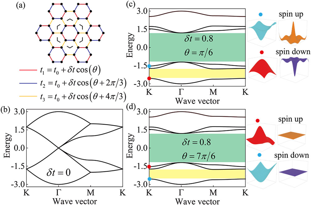
    Fig. 1. Tight-binding model band structures and Berry curvature. (a) Kekulé tight-binding model with intra-cell coupling t1=t0+δtcos(θ), t2=t0+δtcos(θ+2π/3) and inter-cell coupling t3=t0+δtcos(θ+4π/3). Here t0 and δt characterize the modulated strengths and θ varies from 0 to 2π. The unit cell is marked by the black dashed lines. (b) Band structure when t0=1 and δt=0. (c), (d) Band structures for the case of δt=0.8, θ=π/6 and δt=0.8, θ=7π/6. The first and second bandgaps are marked by yellow and green shaded areas, respectively. Right panel: Berry curvatures around K (first column) and Γ point (second column).
    Geometry, band dispersion, and mode patterns of the Kekulé photonic crystal. (a) Unit cell of the structure where a is the lattice constant, r and h are the radius and height of the metallic rods, l is the length of the triangle patches, and wi (i=1,2,3) are the widths of the connecting strips. (b) Band structure for d=0 mm (equivalent connecting strips) and a=21 mm, r=1.2 mm, h=3.2 mm, l=6.5 mm. (c) Band structure when changing d=1.8 mm and θ=π/6 for the geometry in (a). Yellow and green shaded areas represent the bandgaps that support valley and pseudo-spin edge states, respectively. (d) Time-averaged Poynting vectors at K valley (red and blue dots) and eigenfields distribution at Γ point (purple and orange dots). (e), (f) The same as in (c) and (d), but with d=1.8 mm and θ=7π/6.
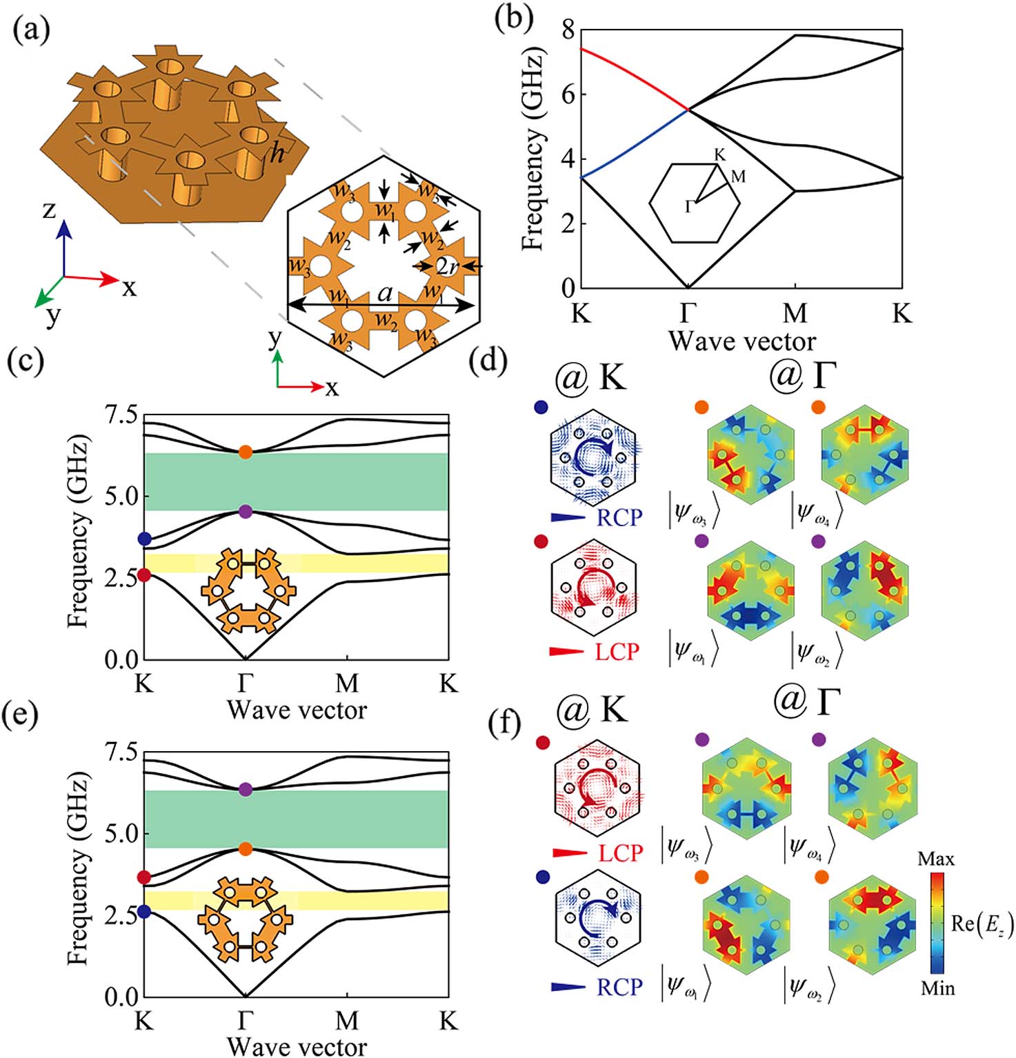
    Fig. 2. Geometry, band dispersion, and mode patterns of the Kekulé photonic crystal. (a) Unit cell of the structure where a is the lattice constant, r and h are the radius and height of the metallic rods, l is the length of the triangle patches, and wi(i=1,2,3) are the widths of the connecting strips. (b) Band structure for d=0  mm (equivalent connecting strips) and a=21  mm, r=1.2  mm, h=3.2  mm, l=6.5  mm. (c) Band structure when changing d=1.8  mm and θ=π/6 for the geometry in (a). Yellow and green shaded areas represent the bandgaps that support valley and pseudo-spin edge states, respectively. (d) Time-averaged Poynting vectors at K valley (red and blue dots) and eigenfields distribution at Γ point (purple and orange dots). (e), (f) The same as in (c) and (d), but with d=1.8  mm and θ=7π/6.
    Projected band structure and the valley edge state transportation. (a) Projected band structure of the supercell composed of two structures with different topological phases splice up (d=1.8 mm, θ=π/6) and down (d=1.8 mm, θ=7π/6). Right panel: the supercell structure and the eigenfield of valley edge states. (b) Measured normalized transmission spectra for edge states propagation for the straight/z-shaped interface (blue and red curves) and bulk region (black curve). The gray area corresponds to the frequency range of edge state. (c), (e) Schemes of straight and z-shaped interface domain walls. The excitation source is placed on the left as the input. (d), (f) Simulated electric fields distribution for straight and z-shaped interface domain walls at f=2.9 GHz.
    Fig. 3. Projected band structure and the valley edge state transportation. (a) Projected band structure of the supercell composed of two structures with different topological phases splice up (d=1.8  mm, θ=π/6) and down (d=1.8  mm, θ=7π/6). Right panel: the supercell structure and the eigenfield of valley edge states. (b) Measured normalized transmission spectra for edge states propagation for the straight/z-shaped interface (blue and red curves) and bulk region (black curve). The gray area corresponds to the frequency range of edge state. (c), (e) Schemes of straight and z-shaped interface domain walls. The excitation source is placed on the left as the input. (d), (f) Simulated electric fields distribution for straight and z-shaped interface domain walls at f=2.9  GHz.
    Projected band structure and pseudo-spin edge state transportation. (a) Projected band structure as a function of θ0 at kx=0. The even and odd symmetry modes of pseudo-spin edge states at θ0=π/2 are shown in the inset, and respectively marked by the red and blue solid lines. The gray shaded regions correspond to bulk modes. Yellow dot represents the degenerate point of edge states with even and odd modes. (b) Projected band structure of supercell comprising structures with θ0=π/9. Spin-up and spin-down edge states are marked in red and blue dashed lines, respectively. (c) Simulated electric fields distribution for straight and z-shaped interface domain walls at f=4.8 GHz. (d) Measured normalized transmission spectra for edge states propagation for the straight/z-shaped interface (blue and red curves) and bulk region (black curve) when placing a point source at left and a receiver at right. The highlight gray region represents the edge states frequencies.
    Fig. 4. Projected band structure and pseudo-spin edge state transportation. (a) Projected band structure as a function of θ0 at kx=0. The even and odd symmetry modes of pseudo-spin edge states at θ0=π/2 are shown in the inset, and respectively marked by the red and blue solid lines. The gray shaded regions correspond to bulk modes. Yellow dot represents the degenerate point of edge states with even and odd modes. (b) Projected band structure of supercell comprising structures with θ0=π/9. Spin-up and spin-down edge states are marked in red and blue dashed lines, respectively. (c) Simulated electric fields distribution for straight and z-shaped interface domain walls at f=4.8  GHz. (d) Measured normalized transmission spectra for edge states propagation for the straight/z-shaped interface (blue and red curves) and bulk region (black curve) when placing a point source at left and a receiver at right. The highlight gray region represents the edge states frequencies.
    Field distributions, Fourier spectra, and k-space out-coupling of edge states into free space. (a) Field distributions of the valley edge state scattered into the free space at f=2.9 GHz. The interface channel consists of the Kekulé lattice with θ=π/6 and θ=7π/6. The dashed red box depicts the measured region in the experiment. (b) Fourier spectra of valley edge states [yellow region in (a)] and k-space analysis of the out-coupling of the valley edge states. (c) The experiment sample and field distributions of the end-scattering of valley edge states at f=2.9 GHz, corresponding to (a). (d) Field distributions of the pseudo-spin edge state scattered into the free space at f=5.5 GHz. The blue arrow represents the scattering direction. (e) Fourier spectra of pseudo-spin edge states [yellow region in (d)] and k-space analysis at the termination boundary of pseudo-spin edge state. (f) Experimentally measured field distributions of the end-scattering of pseudo-spin edge states at f=5.5 GHz.
    Fig. 5. Field distributions, Fourier spectra, and k-space out-coupling of edge states into free space. (a) Field distributions of the valley edge state scattered into the free space at f=2.9  GHz. The interface channel consists of the Kekulé lattice with θ=π/6 and θ=7π/6. The dashed red box depicts the measured region in the experiment. (b) Fourier spectra of valley edge states [yellow region in (a)] and k-space analysis of the out-coupling of the valley edge states. (c) The experiment sample and field distributions of the end-scattering of valley edge states at f=2.9  GHz, corresponding to (a). (d) Field distributions of the pseudo-spin edge state scattered into the free space at f=5.5  GHz. The blue arrow represents the scattering direction. (e) Fourier spectra of pseudo-spin edge states [yellow region in (d)] and k-space analysis at the termination boundary of pseudo-spin edge state. (f) Experimentally measured field distributions of the end-scattering of pseudo-spin edge states at f=5.5  GHz.
    Discretization of the BZ. Inset: zoom-in of the single plaquette.
    Fig. 6. Discretization of the BZ. Inset: zoom-in of the single plaquette.
    Berry curvature around Γ for topological pseudo-spin channels. (a), (b) Pseudo-spin-up and pseudo-spin-down Berry curvatures for the case of δt=0.8, θ=π/6. (c), (d) The same as in (a) and (b) but with δt=0.8, θ=7π/6.
    Fig. 7. Berry curvature around Γ for topological pseudo-spin channels. (a), (b) Pseudo-spin-up and pseudo-spin-down Berry curvatures for the case of δt=0.8, θ=π/6. (c), (d) The same as in (a) and (b) but with δt=0.8, θ=7π/6.
    Evolution of operator A to the eigenstates at ∠k=π/6 (|k|=0.06π/3a).
    Fig. 8. Evolution of operator A to the eigenstates at k=π/6 (|k|=0.06π/3a).
    Topological edge states propagate in multi-channel structures. (a)–(c) Schematic of finite structures with different interface channel angles. The pink and green structures represent the distorted Kekulé lattice with θ=π/6 and θ=7π/6, respectively. Interface channels are marked by yellow regions. (d)–(f) Electric field distributions of valley edge states at f=2.9 GHz. (g)–(i) Electric field distributions of pseudo-spin edge states at f=4.8 GHz. The orange arrows represent the propagation direction.
    Fig. 9. Topological edge states propagate in multi-channel structures. (a)–(c) Schematic of finite structures with different interface channel angles. The pink and green structures represent the distorted Kekulé lattice with θ=π/6 and θ=7π/6, respectively. Interface channels are marked by yellow regions. (d)–(f) Electric field distributions of valley edge states at f=2.9  GHz. (g)–(i) Electric field distributions of pseudo-spin edge states at f=4.8  GHz. The orange arrows represent the propagation direction.
    Field distributions of valley and pseudo-spin edge states. (a), (b) Propagation of valley edge states when a circularly polarized source with the frequency of f=2.9 GHz is placed in the middle of the interface channel. (c), (d) The same as in (a) and (b) but the operating frequency is switched to f=4.9 GHz. Inset: the arrangement of the four-dipole source array and the electric field of circularly polarized source, LCP in (a), RCP in (b).
    Fig. 10. Field distributions of valley and pseudo-spin edge states. (a), (b) Propagation of valley edge states when a circularly polarized source with the frequency of f=2.9  GHz is placed in the middle of the interface channel. (c), (d) The same as in (a) and (b) but the operating frequency is switched to f=4.9  GHz. Inset: the arrangement of the four-dipole source array and the electric field of circularly polarized source, LCP in (a), RCP in (b).
    Field distributions and k-space out-coupling of edge states into free space. (a), (b) Field distributions of the valley edge state in different interface channels at f=2.9 GHz. (c) k-space analysis of the out-coupling of the valley edge states. BZ, dispersion of air, and termination are represented by the black hexagonal boxes, black circle, and green dashed line. (d), (e) Field distributions of the pseudo-spin edge state in different channels at f=5.5 GHz. The red arrow represents the scattering direction. (f) k-space analysis at the termination boundary of the pseudo-spin edge state.
    Fig. 11. Field distributions and k-space out-coupling of edge states into free space. (a), (b) Field distributions of the valley edge state in different interface channels at f=2.9  GHz. (c) k-space analysis of the out-coupling of the valley edge states. BZ, dispersion of air, and termination are represented by the black hexagonal boxes, black circle, and green dashed line. (d), (e) Field distributions of the pseudo-spin edge state in different channels at f=5.5  GHz. The red arrow represents the scattering direction. (f) k-space analysis at the termination boundary of the pseudo-spin edge state.
    Guochao Wei, Zhenzhen Liu, Licheng Wang, Jianyuan Song, Jun-Jun Xiao. Coexisting valley and pseudo-spin topological edge states in photonic topological insulators made of distorted Kekulé lattices[J]. Photonics Research, 2022, 10(4): 999
    Download Citation