• Photonics Research
  • Vol. 10, Issue 4, 999 (2022)
Guochao Wei1, Zhenzhen Liu1, Licheng Wang1, Jianyuan Song2, and Jun-Jun Xiao1、*
Author Affiliations
  • 1Shenzhen Engineering Laboratory of Aerospace Detection and Imaging, College of Electronic and Information Engineering, Harbin Institute of Technology (Shenzhen), Shenzhen 518055, China
  • 2Shenzhen Suntak Multilayer PCB Co., Ltd., Shenzhen 518115, China
  • show less
    DOI: 10.1364/PRJ.453803 Cite this Article Set citation alerts
    Guochao Wei, Zhenzhen Liu, Licheng Wang, Jianyuan Song, Jun-Jun Xiao. Coexisting valley and pseudo-spin topological edge states in photonic topological insulators made of distorted Kekulé lattices[J]. Photonics Research, 2022, 10(4): 999 Copy Citation Text show less

    Abstract

    Photonic topological insulators protected by the lattice spatial symmetry (e.g., inversion and rotation symmetry) mainly support single type edge state, interpreted by either valley or pseudo-spin. Here, we demonstrate theoretically, numerically, and experimentally that a type of judiciously designed two-dimensional Kekulé photonic crystal with time reversal symmetry can possess topological valley and pseudo-spin edge states in different frequency bands. Topologically robust transportation of both the valley and pseudo-spin edge states was confirmed by measuring the transmission of straight and z-shaped interface supported edge mode and comparing with bulk modes in the microwave frequency regime. In addition, we show that due to the distinct topological origins, valley and pseudo-spin edge states can be distinguished by examining their end-scattering into the free space. Our system provides an alternative way in manipulating electromagnetic waves with additional degree-of-freedom, which has potential applications for robust and high-capacity waveguiding and multi-mode dividing.

    1. INTRODUCTION

    One of the most striking topological phenomena in classical wave systems is the support of topological edge states (TESs), which are unidirectional, robust against perturbations, and backscattering immune [111]. Recent studies of TESs are mainly divided into valley and pseudo-spin types [1215]. The former type requires a pair of degenerate but nonequivalent energy extrema in the momentum space, named valley [1625]. The latter is often manifested by a linear band crossing constructed by two degenerate eigenstate pairs [2632]. To extend the degree of freedom of TESs in one specific system, it is possible to combine valley and pseudo-spin photonic topological crystals, resulting in pseudo-spin-valley coupled edge states [33]. However, in all these scenarios, once the structure is constructed, the interface channel only supports a single type edge state, e.g., either the valley edge state (VES) [34], pseudo-spin edge state (PES) [35], or pseudo-spin-valley coupled edge state [33]. This obviously limits the application in multi-band and multi-model on-chip signal processing and communications. In this regard, it is interesting and useful to construct an interface channel that simultaneously supports VESs and PESs within different bandgaps, which can definitely further increase the capacity and the supported topological modes in the specific interface channel. Chen et al. have proposed using interlacing triangular lattices to achieve the coexistence of VESs and PESs [36].

    In this work, we theoretically, numerically, and experimentally demonstrate a quasi-2D lattice system that simultaneously supports VESs and PESs in different frequency bandgaps. The lattice is of the Kekulé type [3740] and made of metallic scatterer covered by two metallic plates. Different from previous studies of multi-band topological edge states guaranteed by the Chern number in a honeycomb ferromagnetic lattice [41] and dual bandgap topological insulators with identical topological origin [4244], the two bandgaps shown here exhibit distinct topological phase transitions, one of which supports VESs and the other hosts a pair of helical edge states describable by the pseudo-spin. We fabricated microwave samples and made both transmission and end-scattering near-field measurements. In regard to the fact that VESs and PESs originate from distinct topological phase transitions, they can be distinguished by the end-scattering direction. Our work may provide an alternative way to realize multi-mode and high-capacity waveguides, which can further promote the applications of topological devices in on-chip communication and signal processing.

    2. MODEL ANALYSIS OF THE DISTORTED KEKULÉ LATTICE

    We first consider a Kekulé-distorted tight-binding model, as shown in Fig. 1(a). The coupling coefficients are t1=t0+δtcos(θ), t2=t0+δtcos(θ+2π/3), and t3=t0+δtcos(θ+4π/3), where t0 and δt characterize the modulated coupling strength and θ varies from 0 to 2π. In the following calculations, we set t0=1 and δt is smaller than t0. The unit cell is marked by the black dashed box, including six sites with equivalent onsite potential. When δt=0, the inter- and intra-cell couplings are t1=t2=t3=t0=1 irrespective of θ. In this case, the chosen unit cell (dashed box) is actually doubling of the primitive unit cell (two nearest neighbor sites), and a four-fold degeneracy appears at Γ due to the band-folding effect, as shown in Fig. 1(b).

    Tight-binding model band structures and Berry curvature. (a) Kekulé tight-binding model with intra-cell coupling t1=t0+δt cos(θ), t2=t0+δt cos(θ+2π/3) and inter-cell coupling t3=t0+δt cos(θ+4π/3). Here t0 and δt characterize the modulated strengths and θ varies from 0 to 2π. The unit cell is marked by the black dashed lines. (b) Band structure when t0=1 and δt=0. (c), (d) Band structures for the case of δt=0.8, θ=π/6 and δt=0.8, θ=7π/6. The first and second bandgaps are marked by yellow and green shaded areas, respectively. Right panel: Berry curvatures around K (first column) and Γ point (second column).

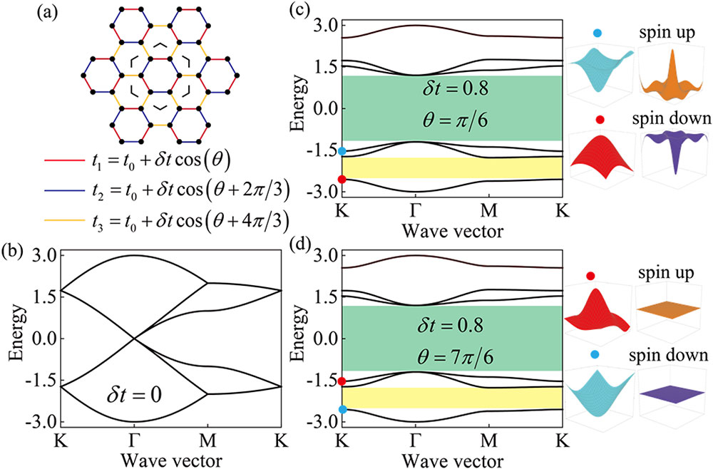
    Figure 1.Tight-binding model band structures and Berry curvature. (a) Kekulé tight-binding model with intra-cell coupling t1=t0+δtcos(θ), t2=t0+δtcos(θ+2π/3) and inter-cell coupling t3=t0+δtcos(θ+4π/3). Here t0 and δt characterize the modulated strengths and θ varies from 0 to 2π. The unit cell is marked by the black dashed lines. (b) Band structure when t0=1 and δt=0. (c), (d) Band structures for the case of δt=0.8, θ=π/6 and δt=0.8, θ=7π/6. The first and second bandgaps are marked by yellow and green shaded areas, respectively. Right panel: Berry curvatures around K (first column) and Γ point (second column).

    To lift up the degenerate points, we consider nonzero δt and θ. In this way, the band-folding effect is broken and the rotation symmetry of the lattice is reduced from C6 to C3, thus resulting in two complete bandgaps around Γ and K points. Figures 1(c) and 1(d) show the band structures for the cases of δt=0.8, θ=π/6 and δt=0.8, θ=7π/6, respectively. They both demonstrate the same dispersion since the two structures can be converted to each other by the rotation operation. To explore the topological properties of each bandgap, the Berry curvatures are calculated (see details in Appendix A) and shown in the right panel around K (first column) and Γ (second column). The corresponding valley (spin) Chern number is calculated by integrating the Berry curvature over the half (whole) irreducible Brillouin zone (BZ). For the valley Hall bandgap (marked by the yellow shaded area), the valley Chern number is CvK=1/2 for δt=0.8, θ=π/6 and CvK=1/2 for δt=0.8, θ=7π/6. We note that the band inversion occurs between the first and the third bands, which is different from previous studies of valley Hall photonic topological insulators where the first and the second bands are switched [34,45]. As for the pseudo-spin bandgap (marked by the green shaded area), the spin Chern number is Cs±=±1 for δt=0.8, θ=π/6 and Cs±=0 for δt=0.8, θ=7π/6. The distinct valley (spin) Chern number indicates that these two structures exhibit different topological phases in the first and second bandgaps.

    3. VALLEY AND PSEUDO-SPIN EDGE STATES: SIMULATION AND MEASUREMENT

    According to the Kekulé tight-binding model, we design a microwave topological insulator which is composed of a hexagon lattice with lattice constant a, as shown in Fig. 2(a). The metallic scatterer is confined between two copper plates and consists of six via holes with diameter r and height h, as well as six triangle patches with side length l at the top. The scatterer is directly connected to the bottom metallic plate, and there is a gap g between the scatterer and the upper metallic plate. The thickness of the copper films is t=0.035  mm and the background material is FR4 of dielectric permittivity ε=4.2. It is worth noting that the widths of the connecting strips are set to wi=w+dcos[θ+(i1)2π/3] for i=1,2,3, where w=2  mm, d and θ are used to modulate the strip widths. When d=0  mm, the widths of the connecting strips are w1=w2=w3=2  mm. In this case, there exists a three-fold degeneracy with frequency f=3.4  GHz at K and a four-fold degeneracy with frequency f=5.5  GHz at Γ point, which are guaranteed by the band-folding effect and C6 rotation symmetry; the corresponding band structure is shown in Fig. 2(b) wherein the blue and red lines represent double degenerated bands.

    Geometry, band dispersion, and mode patterns of the Kekulé photonic crystal. (a) Unit cell of the structure where a is the lattice constant, r and h are the radius and height of the metallic rods, l is the length of the triangle patches, and wi (i=1,2,3) are the widths of the connecting strips. (b) Band structure for d=0 mm (equivalent connecting strips) and a=21 mm, r=1.2 mm, h=3.2 mm, l=6.5 mm. (c) Band structure when changing d=1.8 mm and θ=π/6 for the geometry in (a). Yellow and green shaded areas represent the bandgaps that support valley and pseudo-spin edge states, respectively. (d) Time-averaged Poynting vectors at K valley (red and blue dots) and eigenfields distribution at Γ point (purple and orange dots). (e), (f) The same as in (c) and (d), but with d=1.8 mm and θ=7π/6.

    Figure 2.Geometry, band dispersion, and mode patterns of the Kekulé photonic crystal. (a) Unit cell of the structure where a is the lattice constant, r and h are the radius and height of the metallic rods, l is the length of the triangle patches, and wi(i=1,2,3) are the widths of the connecting strips. (b) Band structure for d=0  mm (equivalent connecting strips) and a=21  mm, r=1.2  mm, h=3.2  mm, l=6.5  mm. (c) Band structure when changing d=1.8  mm and θ=π/6 for the geometry in (a). Yellow and green shaded areas represent the bandgaps that support valley and pseudo-spin edge states, respectively. (d) Time-averaged Poynting vectors at K valley (red and blue dots) and eigenfields distribution at Γ point (purple and orange dots). (e), (f) The same as in (c) and (d), but with d=1.8  mm and θ=7π/6.

    It is well known that by shrinking or expending the honeycomb lattice, the four-fold degeneracy at the Γ point would evolve into a pair of double degenerate points, thus opening a bandgap around the degeneracy frequency. However, under the same operations, the degenerate point at the K valley persists, which is protected by the C6 rotation symmetry [46]. Here, in order to simultaneously break the three-fold degeneracy at K and the four-fold one at Γ, we consider the nonzero modulated strength d. This reduces the rotation symmetry of the Kekulé lattice from C6 to C3. Consequently, these two degenerate points can be both lifted up, resulting in two complete bandgaps. Figures 2(c) and 2(e) show the band structures for d=1.8  mm, θ=π/6 and d=1.8  mm, θ=7π/6, respectively. As expected, two bandgaps show up and are respectively ranged from f=2.6  GHz to f=3.41  GHz (marked by the yellow shaded area), and f=4.5  GHz to f=6.3  GHz (marked by the green shaded area). We note that in this distorted Kekulé lattice with C3 rotation symmetry, the double degeneracy at Γ is guaranteed by the synthetic Kramers pairs (A=KUC3) rather than the C6 rotation symmetry in breathing honeycomb lattice [39] (see more details in Appendix B).

    To clarify the topological properties associated with each bandgap, we calculate the time-averaged Poynting vectors at K point and the eigenfield Re(Ez) at Γ point by COMSOL Multiphysics [47]. The results are shown in Fig. 2(d) (d=1.8  mm and θ=π/6) and Fig. 2(f) (d=1.8  mm and θ=7π/6). The time-averaged Poynting vectors and eigenfield patterns are respectively switched in these two cases, indicating the distinct topological properties. Note that, at Γ point, if the lattice has C6 rotation symmetry, the 2D representations E1 and E2 are isomorphic to the px/py orbitals and dx2y2/dxy orbitals [26]. However, here in our considered distorted Kekulé lattice, since the inversion symmetry of the unit cell is broken, these two kinds of eigenstates are mixed with each other and are labeled as |ψω1, |ψω2, |ψω3, and |ψω4, respectively.

    To explore the VESs numerically, we construct the supercell [shown in the center panel in Fig. 3(a)] composed of the two typical structures with d=1.8  mm, θ=θ0 at the upper part and d=1.8  mm, θ=θ0+π at the lower part. Figure 3(a) shows the projected band for the periodic structure made of this supercell when θ0=π/6. It is seen that a VES (marked by the black curve) lies in the first bandgap. It is expected that VESs at different valleys (K/K) shall go in the opposite propagation direction, exhibiting the valley-locked chirality (see more details in Appendix C) [45]. Here, without loss of generality, we have focused on the VES projected at the K valley. The simulated Ez component of the edge state is shown in the panel right to Fig. 3(a). It is seen that the electromagnetic field is well confined around the interface and strongly decays into the bulk in the transverse direction.

    Projected band structure and the valley edge state transportation. (a) Projected band structure of the supercell composed of two structures with different topological phases splice up (d=1.8 mm, θ=π/6) and down (d=1.8 mm, θ=7π/6). Right panel: the supercell structure and the eigenfield of valley edge states. (b) Measured normalized transmission spectra for edge states propagation for the straight/z-shaped interface (blue and red curves) and bulk region (black curve). The gray area corresponds to the frequency range of edge state. (c), (e) Schemes of straight and z-shaped interface domain walls. The excitation source is placed on the left as the input. (d), (f) Simulated electric fields distribution for straight and z-shaped interface domain walls at f=2.9 GHz.

    Figure 3.Projected band structure and the valley edge state transportation. (a) Projected band structure of the supercell composed of two structures with different topological phases splice up (d=1.8  mm, θ=π/6) and down (d=1.8  mm, θ=7π/6). Right panel: the supercell structure and the eigenfield of valley edge states. (b) Measured normalized transmission spectra for edge states propagation for the straight/z-shaped interface (blue and red curves) and bulk region (black curve). The gray area corresponds to the frequency range of edge state. (c), (e) Schemes of straight and z-shaped interface domain walls. The excitation source is placed on the left as the input. (d), (f) Simulated electric fields distribution for straight and z-shaped interface domain walls at f=2.9  GHz.

    To justify the robustness of the VES, we designed two samples with a typical domain wall routing scheme, e.g., the straight [Fig. 3(c)] and the z-shaped [Fig. 3(e)] edge channels. Figures 3(d) and 3(f) illustrate the simulated electric field distributions of the VESs propagating along the straight and the z-shaped interfaces at f=2.9  GHz. As can be seen, waves are well confined around the interface channel and propagate smoothly despite encountering two sharp bending corners, which demonstrates the highly suppressed backscattering and nearly reflectionless propagation. Furthermore, the unidirectional transportation of the TES is shown in Appendix D.

    To quantitatively analyze the transmission property of the VES, we fabricated the two samples with printed circuit board technology and experimentally measured the normalized transmission for straight interface (blue curve), z-shaped interface (red curve), and bulk modes (black curve). The results are plotted in Fig. 3(b) which shows that the normalized transmission of the z-shaped interface is close to that of the straight interface, indicating the robust propagation against the sharp bending of the domain wall channel. The gray area in Fig. 3(b) represents the frequency range of the VESs. Slight difference with respect to the simulation results in Fig. 3(a) (black curve covered frequency range) is ascribed to possible fabrication inaccuracy.

    To examine the PESs, we focus on the second bandgap. The supercell structure is basically the same as that in Fig. 3(a), but with θ0 varying from 0 to π. The corresponding bulk bands and edge states at kx=0 are shown in Fig. 4(a). The red and blue dashed lines represent the PESs of the even and odd symmetry with respect to the y axis [field distributions for the case of θ0=π/2 are shown in the inset of Fig. 4(a)]. Note that these two PESs (spin-up and spin-down) are degenerated at θ0=π/9 (marked by the yellow dot), which is not observed in previously studied photonic topological insulators with C6 rotation symmetry due to the absence of half-integer total spin [39].

    Projected band structure and pseudo-spin edge state transportation. (a) Projected band structure as a function of θ0 at kx=0. The even and odd symmetry modes of pseudo-spin edge states at θ0=π/2 are shown in the inset, and respectively marked by the red and blue solid lines. The gray shaded regions correspond to bulk modes. Yellow dot represents the degenerate point of edge states with even and odd modes. (b) Projected band structure of supercell comprising structures with θ0=π/9. Spin-up and spin-down edge states are marked in red and blue dashed lines, respectively. (c) Simulated electric fields distribution for straight and z-shaped interface domain walls at f=4.8 GHz. (d) Measured normalized transmission spectra for edge states propagation for the straight/z-shaped interface (blue and red curves) and bulk region (black curve) when placing a point source at left and a receiver at right. The highlight gray region represents the edge states frequencies.

    Figure 4.Projected band structure and pseudo-spin edge state transportation. (a) Projected band structure as a function of θ0 at kx=0. The even and odd symmetry modes of pseudo-spin edge states at θ0=π/2 are shown in the inset, and respectively marked by the red and blue solid lines. The gray shaded regions correspond to bulk modes. Yellow dot represents the degenerate point of edge states with even and odd modes. (b) Projected band structure of supercell comprising structures with θ0=π/9. Spin-up and spin-down edge states are marked in red and blue dashed lines, respectively. (c) Simulated electric fields distribution for straight and z-shaped interface domain walls at f=4.8  GHz. (d) Measured normalized transmission spectra for edge states propagation for the straight/z-shaped interface (blue and red curves) and bulk region (black curve) when placing a point source at left and a receiver at right. The highlight gray region represents the edge states frequencies.

    Figure 4(b) shows the band structures for the case of θ0=π/9. Two PESs of spin-up (marked by the red curve) and spin-down (marked by the blue curve) modes are present within the bandgap from f=4.4  GHz to f=6.26  GHz. To demonstrate the strongly suppressed backscattering in the sharp bending case, we numerically simulated the electric fields and experimentally measured the corresponding transmission. The finite structures with straight and z-shaped interfaces are the same as in Figs. 3(c) and 3(e), but the operating frequency here is switched to f=4.8  GHz. Figure 4(c) illustrates the field distributions. Similar to the VESs, the two sharp bends have almost negligible effect on the propagation of the PESs. Figure 4(d) shows the measured transmission spectra of the straight/z-shaped interface and bulk modes. The transmissions of the straight and the z-shaped interface channels are almost coincided, as expected.

    4. REFRACTION OF VALLEY AND PSEUDO-SPIN TOPOLOGICAL EDGE STATES

    So far, we have shown that the VESs and PESs exhibit topologically protected transportation properties (e.g., being almost unidirectional and backscattering immune) along the topological interface. It is difficult to distinguish the edge states only by comparing the transmission efficiency and electric field distribution. Here we show that the two types of edge modes have remarkably different end-scattering into free space due to the distinct topological origins. Figure 5 shows both the numerical and experimental results for end-scattering in a finite structure with a straight interface channel composed of Kekulé lattice with θ=π/6 (upper part) and θ=7π/6 (lower part). We emphasize that the VES in this structure is at extremely low frequencies (around f=2.9  GHz). At this frequency, the Bloch wave vector at K/K point is kΓK=4π/3a=199.5  m1 while that in air is k0=2πf/c=60.7  m1. Apparently, the VESs cannot be scattered into the free space due to the strong wave vector mismatch (k0kΓK).

    Field distributions, Fourier spectra, and k-space out-coupling of edge states into free space. (a) Field distributions of the valley edge state scattered into the free space at f=2.9 GHz. The interface channel consists of the Kekulé lattice with θ=π/6 and θ=7π/6. The dashed red box depicts the measured region in the experiment. (b) Fourier spectra of valley edge states [yellow region in (a)] and k-space analysis of the out-coupling of the valley edge states. (c) The experiment sample and field distributions of the end-scattering of valley edge states at f=2.9 GHz, corresponding to (a). (d) Field distributions of the pseudo-spin edge state scattered into the free space at f=5.5 GHz. The blue arrow represents the scattering direction. (e) Fourier spectra of pseudo-spin edge states [yellow region in (d)] and k-space analysis at the termination boundary of pseudo-spin edge state. (f) Experimentally measured field distributions of the end-scattering of pseudo-spin edge states at f=5.5 GHz.

    Figure 5.Field distributions, Fourier spectra, and k-space out-coupling of edge states into free space. (a) Field distributions of the valley edge state scattered into the free space at f=2.9  GHz. The interface channel consists of the Kekulé lattice with θ=π/6 and θ=7π/6. The dashed red box depicts the measured region in the experiment. (b) Fourier spectra of valley edge states [yellow region in (a)] and k-space analysis of the out-coupling of the valley edge states. (c) The experiment sample and field distributions of the end-scattering of valley edge states at f=2.9  GHz, corresponding to (a). (d) Field distributions of the pseudo-spin edge state scattered into the free space at f=5.5  GHz. The blue arrow represents the scattering direction. (e) Fourier spectra of pseudo-spin edge states [yellow region in (d)] and k-space analysis at the termination boundary of pseudo-spin edge state. (f) Experimentally measured field distributions of the end-scattering of pseudo-spin edge states at f=5.5  GHz.

    Figure 5(a) shows the full-wave simulation results for a sloping termination boundary between the finite structure and free space. Specifically, a point source with frequency f=2.9  GHz is located at the left side of the channel to excite the VESs. As can be seen, a small amount of energy can be scattered into the free space when the propagating edge mode encounters the termination boundary. Note that partially scattered waves propagate along the interface between θ=π/6 and free space, mainly due to the existence of the chiral edge state guaranteed by distinct valley Chern numbers, Kekulé-distorted lattice (CvK=1/2), and free space (CvK=0) [48,49]. Moreover, the boundary states are highly related to the shape of the terminations [50].

    To understand the end-scattering phenomenon, the corresponding Fourier transform of VESs field pattern [region framed by the yellow rectangle in Fig. 5(a)] and the k-space analysis of out-coupling at the sloping termination are shown in Fig. 5(b). In the spatial Fourier spectra, only three corners of the BZ are dominantly bright, corresponding to one specific valley (K). In contrast, the three dark corners of the BZ indicate that the opposite valley (K) components are heavily suppressed, which suggests that only the edge state associated with K valley is excited. In the k-space analysis superimposed in Fig. 5(b), the green hexagonal boxes, yellow dashed circle, and green dashed line represent the BZ of the sample lattice, the 2.9 GHz air dispersion circle, and the termination boundary of the sample, respectively. The gray dashed lines perpendicular to the boundary interface mark the possible scattering channels for Bloch harmonics that may conserve the parallel momentum. However, due to the mismatch (no-intersection) between the gray dashed lines and the yellow dashed circle in the BZ center, VESs cannot be refracted directly from the interface termination into free space. We note that when considering different lattice constant “a” by expanding (shrinking) the lattice which, however, also decreases (increases) the operating frequency while shrinking (expanding) the BZ of the lattice, there is still no-intersection between the allowed scattering channels among the VES Bloch harmonics and the air dispersion. Figure 5(c) shows the fabricated sample and measured electric fields corresponding to Fig. 5(a). The topological interface channel is marked by the red dashed line and the measured region is marked by the red dashed box. As can be seen, little energy can be scattered from the sloping termination boundary into free space, which is coincident with Fig. 5(a).

    Figure 5(d) shows the refraction situation of the PESs at f=5.5  GHz. Compared with the VESs [as shown in Fig. 5(a)], waves propagate along the normal direction (blue arrow) of the boundary upon escaping from the interface guiding channel. Again, we calculate the Fourier transform of the PES field [yellow region in Fig. 5(d)], and the parallel-momentum-matching condition at the sloping termination is shown in Fig. 5(e). We can see that the spatial Fourier spectra are bright at the centers of BZ, indicating the PES excitation is mainly dominated by the Γ point modes. In this way, the gray dashed line connecting two Γ points represents the parallel wave vector conservation condition (in this case k=0). The corresponding refraction direction is marked by the blue arrow for the normal of the termination (green dashed line). We remark that in this case the refraction direction of PES is independent of the operating frequency due to the fact that at each operating frequency, the PES wave vector always intersects with the air equal-frequency contour (see more details in Appendix E) [51]. Figure 5(f) shows the measured end-scattering fields at 5.5 GHz. Clearly, the end-scattering direction (marked by the blue arrow) is perpendicular to the sloping termination, which is in good agreement with Fig. 5(d).

    5. CONCLUSION

    In summary, we theoretically, numerically, and experimentally investigate the coexistence of topological VESs and PESs in a microwave substrate-integrated distorted Kekulé metastructure. By comparing the full-wave simulations and the experimental measurements, both the VESs and PESs in the system are verified robust to sharp bends. In addition, to observably distinguish VESs and PESs, we measure the scattered electric fields of the edge states into free space and present out-coupling mechanism analysis based on the corresponding Fourier spectra. The microwave distorted Kekulé lattice might be extended to optical frequencies based on the dielectric slab system. To confine the waves at the interface channel with little radiation, one may optimize appreciable nontrivial bandgaps that fall below the light cone. Our work provides a way to design topological devices for multi-band and multi-model distinguished topological waveguides within one specific system.

    APPENDIX A: TIGHT-BINDING MODEL OF THE KEKULé LATTICE

    The corresponding Hamiltonian of the Kekulé tight-binding model in Fig. 1(a) reads H=(0t20t3ei(kx2+3ky2)0t1t20t10t3eikx00t10t20t3ei(kx2+3ky2)t3ei(kx2+3ky2)0t20t100t3eikx0t10t2t10t3ei(kx23ky2)0t20),where t1=t0+δtcos(θ), t2=t0+δtcos(θ+2π/3), and t3=t0+δtcos(θ+4π/3). To understand the topological properties of the first bandgap, the Berry curvature around the K valley can be calculated directly by using the discrete method. Figure 6 shows the discretization of the BZ. The Berry curvature of each plaquette is given by [52] Ω(k)=ln(uk1|uk2uk2|uk3uk4|uk3uk1|uk4),where |uk1=|uk, |uk2=|uk+δk1, |uk3=|uk+δk1+δk2, and |uk4=|uk+δk2 are the periodic wave functions. Then the valley Chern number can be calculated as Cv=HBZΩ(k)dS,where HBZ represents the half of the BZ.

    Discretization of the BZ. Inset: zoom-in of the single plaquette.

    Figure 6.Discretization of the BZ. Inset: zoom-in of the single plaquette.

    Berry curvature around Γ for topological pseudo-spin channels. (a), (b) Pseudo-spin-up and pseudo-spin-down Berry curvatures for the case of δt=0.8, θ=π/6. (c), (d) The same as in (a) and (b) but with δt=0.8, θ=7π/6.

    Figure 7.Berry curvature around Γ for topological pseudo-spin channels. (a), (b) Pseudo-spin-up and pseudo-spin-down Berry curvatures for the case of δt=0.8, θ=π/6. (c), (d) The same as in (a) and (b) but with δt=0.8, θ=7π/6.

    As a comparison, we also considered the system with δt=0.8 and θ=7π/6. In this case, H+(k)=H(k)=(0.920.16(kx2+ky2)0.77+0.19(kx2+ky2)0.77+0.19(kx2+ky2)0.92+0.16(kx2+ky2)),and the Berry curvatures are shown in Figs. 7(c) and 7(d). The corresponding spin Chern numbers are Cs±=0, which demonstrate the trivial topological phase of the second bandgap.

    APPENDIX B: SYNTHETIC KRAMERS PAIR

    The double degeneracy at Γ point in the Kekulé-distorted 2D lattice is guaranteed by the synthetic Kramers pair, A2=C32(A=KUC3) [39]. Here, K and C3 are the complex conjugate and rotation operators, respectively, and U=(0100100000010010)is the unitary operator. First, we examine the four eigenstates (structure with d=1.8  mm, θ=7π/6) around Γ point along the π/6 azimuth angle (ΓM direction with |k|=0.06π/3a) in momentum space; the corresponding electric fields [Re(Ez)] are shown in the first column in Fig. 8. Starting from the eigenstates in the first column, K operator maps the wave function to their time-reversed counterpart. U operator swaps the wave functions as |ω1|ω2, |ω2|ω1, |ω3|ω4, and |ω4|ω3. C3 operator rotates each wave function about 2π/3 clockwise. Comparing the first and the last columns in Fig. 8, one can get A2|ψ=C32|ψ.

    Evolution of operator A to the eigenstates at ∠k=π/6 (|k|=0.06π/3a).

    Figure 8.Evolution of operator A to the eigenstates at k=π/6 (|k|=0.06π/3a).

    APPENDIX C: VALLEY AND PSEUDO-SPIN LOCKED EDGE STATES

    The topological edge mode only travels along the interface with the same valley or pseudo-spin degree of freedom. To show that, we construct three types of finite structures with different interface angles, as shown in Figs. 9(a)–9(c). A point source is placed at the left side of the interface, and the full-wave simulated electric fields at different frequencies are shown in Figs. 9(d)–9(i). Apparently, the wave cannot go straightforward to the right-side output because of topological edge mode mismatching.

    Topological edge states propagate in multi-channel structures. (a)–(c) Schematic of finite structures with different interface channel angles. The pink and green structures represent the distorted Kekulé lattice with θ=π/6 and θ=7π/6, respectively. Interface channels are marked by yellow regions. (d)–(f) Electric field distributions of valley edge states at f=2.9 GHz. (g)–(i) Electric field distributions of pseudo-spin edge states at f=4.8 GHz. The orange arrows represent the propagation direction.

    Figure 9.Topological edge states propagate in multi-channel structures. (a)–(c) Schematic of finite structures with different interface channel angles. The pink and green structures represent the distorted Kekulé lattice with θ=π/6 and θ=7π/6, respectively. Interface channels are marked by yellow regions. (d)–(f) Electric field distributions of valley edge states at f=2.9  GHz. (g)–(i) Electric field distributions of pseudo-spin edge states at f=4.8  GHz. The orange arrows represent the propagation direction.

    APPENDIX D: UNIDIRECTIONAL TRANSPORTATION OF VALLEY AND PSEUDO-SPIN EDGE STATES

    One of the most important properties of the topological edge state (valley or pseudo-spin) is the unidirectional transportation. Figure 10 shows the electric field (|Ez|) distributions for the valley (f=2.9  GHz) and pseudo-spin edge states (f=4.9  GHz) when the circularly polarized source (red and yellow stars) is placed in the middle of the interface channel. The finite structure is the same as in Fig. 3(a). As can be seen, waves almost propagate along a particular direction. Little energy couples to the opposite direction due to the imperfection of the circularly polarized source composed of a four-dipole source array with the phase varying clockwise (anticlockwise) by π/4. The arrangement of the four-dipole source array and the corresponding electric fields are shown in the inset of Figs. 10(a) and 10(b).

    Field distributions of valley and pseudo-spin edge states. (a), (b) Propagation of valley edge states when a circularly polarized source with the frequency of f=2.9 GHz is placed in the middle of the interface channel. (c), (d) The same as in (a) and (b) but the operating frequency is switched to f=4.9 GHz. Inset: the arrangement of the four-dipole source array and the electric field of circularly polarized source, LCP in (a), RCP in (b).

    Figure 10.Field distributions of valley and pseudo-spin edge states. (a), (b) Propagation of valley edge states when a circularly polarized source with the frequency of f=2.9  GHz is placed in the middle of the interface channel. (c), (d) The same as in (a) and (b) but the operating frequency is switched to f=4.9  GHz. Inset: the arrangement of the four-dipole source array and the electric field of circularly polarized source, LCP in (a), RCP in (b).

    APPENDIX E: END-SCATTERING OF VALLEY AND PSEUDO-SPIN EDGE STATES

    We have demonstrated the refraction direction of both valley and pseudo-spin edge states at the termination with a 120 deg sloping angle in the main text. To further examine the end-scattering properties, we construct two types of the infinite structures with opposite geometrical configuration where a 60 deg sloping termination boundary is located at the right side. Figures 11(a) and 11(b) show the valley edge states distribution at f=2.9  GHz. Similar to Fig. 5(a), little energy scatters into the free space due to the mismatch between the interface channel and the free space. The corresponding k-space analysis of the out-coupling is shown in Fig. 11(c). As for pseudo-spin edge states, the electric field distributions at f=5.5  GHz are shown in Figs. 11(d) and 11(e). Two types of the interface exhibit the same scattering direction (marked in red arrow). Again, the k-space analysis of the out-coupling is shown in Fig. 11(f).

    Field distributions and k-space out-coupling of edge states into free space. (a), (b) Field distributions of the valley edge state in different interface channels at f=2.9 GHz. (c) k-space analysis of the out-coupling of the valley edge states. BZ, dispersion of air, and termination are represented by the black hexagonal boxes, black circle, and green dashed line. (d), (e) Field distributions of the pseudo-spin edge state in different channels at f=5.5 GHz. The red arrow represents the scattering direction. (f) k-space analysis at the termination boundary of the pseudo-spin edge state.

    Figure 11.Field distributions and k-space out-coupling of edge states into free space. (a), (b) Field distributions of the valley edge state in different interface channels at f=2.9  GHz. (c) k-space analysis of the out-coupling of the valley edge states. BZ, dispersion of air, and termination are represented by the black hexagonal boxes, black circle, and green dashed line. (d), (e) Field distributions of the pseudo-spin edge state in different channels at f=5.5  GHz. The red arrow represents the scattering direction. (f) k-space analysis at the termination boundary of the pseudo-spin edge state.

    References

    [1] A. B. Khanikaev, S. H. Mousavi, W. K. Tse, M. Kargarian, A. H. MacDonald, G. Shvets. Photonic topological insulators. Nat. Mater., 12, 233-239(2013).

    [2] J. Lu, C. Qiu, L. Ye, X. Fan, M. Ke, F. Zhang, Z. Liu. Observation of topological valley transport of sound in sonic crystals. Nat. Phys., 13, 369-374(2016).

    [3] L. Zhang, Y. Yang, M. He, H. X. Wang, Z. Yang, E. Li, F. Gao, B. Zhang, R. Singh, J. H. Jiang, H. Chen. Valley kink states and topological channel intersections in substrate-integrated photonic circuitry. Laser Photonics Rev., 13, 1900159(2019).

    [4] Q. Guo, B. Yang, L. Xia, W. Gao, H. Liu, J. Chen, Y. Xiang, S. Zhang. Three dimensional photonic Dirac points in metamaterials. Phys. Rev. Lett., 119, 213901(2017).

    [5] B. Yang, Q. Guo, B. Tremain, L. E. Barr, W. Gao, H. Liu, B. Beri, Y. Xiang, D. Fan, A. P. Hibbins, S. Zhang. Direct observation of topological surface-state arcs in photonic metamaterials. Nat. Commun., 8, 97(2017).

    [6] W. Gao, M. Lawrence, B. Yang, F. Liu, F. Fang, B. Beri, J. Li, S. Zhang. Topological photonic phase in chiral hyperbolic metamaterials. Phys. Rev. Lett., 114, 037402(2015).

    [7] M. Li, Y. Wang, T. Sang, H. Chu, Y. Lai, G. Yang. Experimental observation of multiple edge and corner states in photonic slabs heterostructures. Photon. Res., 10, 197-204(2021).

    [8] L. Lu, J. D. Joannopoulos, M. Soljačić. Topological photonics. Nat. Photonics, 8, 821-829(2014).

    [9] A. B. Khanikaev, G. Shvets. Two-dimensional topological photonics. Nat. Photonics, 11, 763-773(2017).

    [10] M. Kim, Z. Jacob, J. Rho. Recent advances in 2D, 3D and higher-order topological photonics. Light Sci. Appl., 9, 130(2020).

    [11] S. Iwamoto, Y. Ota, Y. Arakawa. Recent progress in topological waveguides and nanocavities in a semiconductor photonic crystal platform. Opt. Mater. Express, 11, 319-337(2021).

    [12] X.-T. He, E.-T. Liang, J.-J. Yuan, H.-Y. Qiu, X.-D. Chen, F.-L. Zhao, J.-W. Dong. A silicon-on-insulator slab for topological valley transport. Nat. Commun., 10, 872(2019).

    [13] M. I. Shalaev, W. Walasik, A. Tsukernik, Y. Xu, N. M. Litchinitser. Robust topologically protected transport in photonic crystals at telecommunication wavelengths. Nat. Nanotechnol., 14, 31-34(2019).

    [14] L. Wang, R.-Y. Zhang, M. Xiao, D. Han, C. T. Chan, W. Wen. The existence of topological edge states in honeycomb plasmonic lattices. New J. Phys., 18, 103029(2016).

    [15] J. Lu, C. Qiu, M. Ke, Z. Liu. Valley vortex states in sonic crystals. Phys. Rev. Lett., 116, 093901(2016).

    [16] L. Ye, C. Qiu, J. Lu, X. Wen, Y. Shen, M. Ke, F. Zhang, Z. Liu. Observation of acoustic valley vortex states and valley-chirality locked beam splitting. Phys. Rev. B, 95, 174106(2017).

    [17] Y. Yang, H. Jiang, Z. H. Hang. Topological valley transport in two-dimensional honeycomb photonic crystals. Sci. Rep., 8, 1588(2018).

    [18] G. Wei, Z. Liu, Y. Liu, D. Zhang, J. Xiao. Frequency selective topological edge wave routing in meta-structures made of cylinders. Opt. Lett., 45, 5608-5611(2020).

    [19] J. Ma, X. Xi, X. Sun. Topological photonic integrated circuits based on valley kink states. Laser Photonics Rev., 13, 1900087(2019).

    [20] S. Arora, T. Bauer, R. Barczyk, E. Verhagen, L. Kuipers. Direct quantification of topological protection in symmetry-protected photonic edge states at telecom wavelengths. Light Sci. Appl., 10, 9(2021).

    [21] M. Wang, W. Zhou, L. Bi, C. Qiu, M. Ke, Z. Liu. Valley-locked waveguide transport in acoustic heterostructures. Nat. Commun., 11, 3000(2020).

    [22] Y. H. Yang, Y. Yamagami, X. B. Yu, P. Pitchappa, J. Webber, B. L. Zhang, M. Fujita, T. Nagatsuma, R. Singh. Terahertz topological photonics for on-chip communication. Nat. Photonics, 14, 446-451(2020).

    [23] X. Xi, K. P. Ye, R. X. Wu. Topological photonic crystal of large valley Chern numbers. Photon. Res., 8, B1-B7(2020).

    [24] J. Lu, C. Qiu, W. Deng, X. Huang, F. Li, F. Zhang, S. Chen, Z. Liu. Valley topological phases in bilayer sonic crystals. Phys. Rev. Lett., 120, 116802(2018).

    [25] L. He, H. Y. Ji, Y. J. Wang, X. D. Zhang. Topologically protected beam splitters and logic gates based on two-dimensional silicon photonic crystal slabs. Opt. Express, 28, 34015-34023(2020).

    [26] L. H. Wu, X. Hu. Scheme for achieving a topological photonic crystal by using dielectric material. Phys. Rev. Lett., 114, 223901(2015).

    [27] L. H. Wu, X. Hu. Topological properties of electrons in honeycomb lattice with detuned hopping energy. Sci. Rep., 6, 24347(2016).

    [28] C. He, X. Ni, H. Ge, X. C. Sun, Y. B. Chen, M. H. Lu, X. P. Liu, Y. F. Chen. Acoustic topological insulator and robust one-way sound transport. Nat. Phys., 12, 1124-1129(2016).

    [29] H. Kagami, T. Amemiya, S. Okada, N. Nishiyama, X. Hu. Topological converter for high-efficiency coupling between Si wire waveguide and topological waveguide. Opt. Express, 28, 33619-33631(2020).

    [30] J. P. Xia, D. Jia, H. X. Sun, S. Q. Yuan, Y. Ge, Q. R. Si, X. J. Liu. Programmable coding acoustic topological insulator. Adv. Mater., 30, 1805002(2018).

    [31] D. A. J. Bisharat, D. F. Sievenpiper. Electromagnetic-dual metasurfaces for topological states along a 1D interface. Laser Photonics Rev., 13, 1900126(2019).

    [32] L. He, W. X. Zhang, X. D. Zhang. Topological all-optical logic gates based on two-dimensional photonic crystals. Opt. Express, 27, 25841-25859(2019).

    [33] Y. Kang, X. Ni, X. Cheng, A. B. Khanikaev, A. Z. Genack. Pseudo-spin-valley coupled edge states in a photonic topological insulator. Nat. Commun., 9, 3029(2018).

    [34] Z. Zhang, Y. Tian, Y. Wang, S. Gao, Y. Cheng, X. Liu, J. Christensen. Directional acoustic antennas based on valley-Hall topological insulators. Adv. Mater., 30, 1803229(2018).

    [35] Y. Yang, Y. F. Xu, T. Xu, H. X. Wang, J. H. Jiang, X. Hu, Z. H. Hang. Visualization of a unidirectional electromagnetic waveguide using topological photonic crystals made of dielectric materials. Phys. Rev. Lett., 120, 217401(2018).

    [36] M. L. N. Chen, L. J. Jiang, Z. Lan, W. E. I. Sha. Coexistence of pseudospin- and valley-Hall-like edge states in a photonic crystal with C3v symmetry. Phys. Rev. Res., 2, 043148(2020).

    [37] Y. Liu, C. S. Lian, Y. Li, Y. Xu, W. Duan. Pseudospins and topological effects of phonons in a Kekule lattice. Phys. Rev. Lett., 119, 255901(2017).

    [38] T.-W. Liu, F. Semperlotti. Nonconventional topological band properties and gapless helical edge states in elastic phononic waveguides with Kekulé distortion. Phys. Rev. B, 100, 214110(2019).

    [39] T. W. Liu, F. Semperlotti. Synthetic Kramers pair in phononic elastic plates and helical edge states on a dislocation interface. Adv. Mater., 33, 2005160(2021).

    [40] X. Wu, Y. Meng, Y. Hao, R. Y. Zhang, J. Li, X. Zhang. Topological corner modes induced by Dirac vortices in arbitrary geometry. Phys. Rev. Lett., 126, 226802(2021).

    [41] P. A. Pantaleon, R. Carrillo-Bastos, Y. Xian. Topological magnon insulator with a Kekule bond modulation. J. Phys. Condens. Matter, 31, 085802(2019).

    [42] Q. Chen, L. Zhang, M. He, Z. Wang, X. Lin, F. Gao, Y. Yang, B. Zhang, H. Chen. Valley-Hall photonic topological insulators with dual-band kink states. Adv. Opt. Mater., 7, 1900036(2019).

    [43] G.-J. Tang, X.-D. Chen, F.-L. Shi, J.-W. Liu, M. Chen, J.-W. Dong. Frequency range dependent topological phases and photonic detouring in valley photonic crystals. Phys. Rev. B, 102, 174202(2020).

    [44] G.-C. Wei, Z.-Z. Liu, D.-S. Zhang, J.-J. Xiao. Frequency dependent wave routing based on dual-band valley-Hall topological photonic crystal. New J. Phys., 23, 023029(2021).

    [45] X. Wu, Y. Meng, J. Tian, Y. Huang, H. Xiang, D. Han, W. Wen. Direct observation of valley-polarized topological edge states in designer surface plasmon crystals. Nat. Commun., 8, 1304(2017).

    [46] Q. Chen, L. Zhang, S. Xu, Z. Wang, E. Li, Y. Yang, H. Chen. Robust waveguiding in substrate-integrated topological photonic crystals. Appl. Phys. Lett., 116, 231106(2020).

    [47] https://cn.comsol.com. https://cn.comsol.com

    [48] X. Xi, J. Ma, S. Wan, C. H. Dong, X. Sun. Observation of chiral edge states in gapped nanomechanical graphene. Sci. Adv., 7, eabe1398(2021).

    [49] M. L. N. Chen, L. Jun Jiang, Z. Lan, W. E. I. Sha. Local orbital-angular-momentum dependent surface states with topological protection. Opt. Express, 28, 14428-14435(2020).

    [50] J. Wang, Y. Huang, W. Chen. Tailoring edge and interface states in topological metastructures exhibiting the acoustic valley Hall effect. Sci. China: Phys., Mech. Astron., 63, 224611(2019).

    [51] H. B. Huang, Z. H. Tan, S. Y. Huo, L. Y. Feng, J. J. Chen, X. Han. Topologically protected zero refraction of elastic waves in pseudospin-Hall phononic crystals. Commun. Phys., 3, 46(2020).

    [52] M. Blanco de Paz, C. Devescovi, G. Giedke, J. J. Saenz, M. G. Vergniory, B. Bradlyn, D. Bercioux, A. García-Etxarri. Tutorial: computing topological invariants in 2D photonic crystals. Adv. Quantum Technol., 3, 1900117(2019).

    [53] B. A. Bernevig, T. L. Hughes, S. C. Zhang. Quantum spin Hall effect and topological phase transition in HgTe quantum wells. Science, 314, 1757-1761(2006).

    Guochao Wei, Zhenzhen Liu, Licheng Wang, Jianyuan Song, Jun-Jun Xiao. Coexisting valley and pseudo-spin topological edge states in photonic topological insulators made of distorted Kekulé lattices[J]. Photonics Research, 2022, 10(4): 999
    Download Citation