
Peng Teng, Tong Zhou, Yonghuan Wang, Ke Zhao, Xiegang Zhu, Xinchun Lai. Electrical transport properties of cerium doped Bi2Te3 thin films grown by molecular beam epitaxy[J]. Journal of Semiconductors, 2021, 42(12): 122902
- Journal of Semiconductors
- Vol. 42, Issue 12, 122902 (2021)
Abstract
1. Introduction
Topological insulators (TIs) are a class of materials with special topological features in energy bands. Due to the topological surface states protected by time reversal symmetry (TRS)[
Compared with transition elements, rare earth (RE) elements could be optional dopant candidates for the following reasons. On one hand, they usually possess larger local magnetic moments than transition elements, which implies the possibility of larger interactions between local magnetic moments from 4f electrons with topological states, and might result in reducing the dopant concentration to achieve the desired strength of magnetic interactions. On the other hand, the trivalent state of RE ions can substitute the trivalent Bi/Sb ions in TIs without changing the charge carrier density[
In this work, we reported the electronic transport properties of Ce-doped Bi2Te3 thin films grown on Al2O3(0001) substrate by molecular beam epitaxy (MBE) with various Ce concentrations. X-ray diffraction (XRD) revealed that Ce atoms substituted the Bi sites, resulting in the chemical formula of (CexBi1–x)2Te3. Electronic transport measurements demonstrated Kondo effect and Fermi liquid behavior of (CexBi1–x)2Te3 at low temperature. Weak anti-localization (WAL) effect that is closely related to the topological properties of TIs is experimentally investigated by magnetic transport measurements and theoretically studied by using the Hikami–Larkin–Nagaoka (HLN) model[
2. Experimental methods
Pristine and Ce-doped Bi2Te3 thin films were grown on an Al2O3(0001) substrate by MBE, following the well-established three temperature methods[
3. Results and discussions
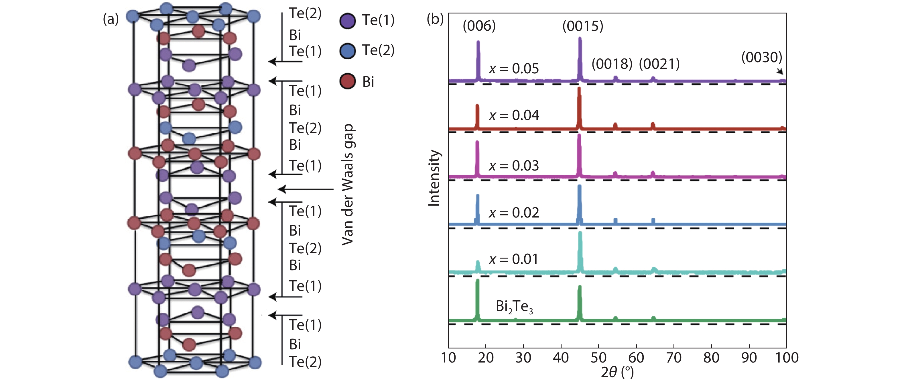
Fig. 1(a) shows the crystal structure of Bi2Te3. Bi2Te3 has a layered hexagonal structure. The smallest repeating unit consists of five atomic layers with a stacking sequence of -Te(1)-Bi-Te(2)-Bi-Te(1)-, which is called a quintuple layer (QL). The interaction between neighboring QLs is the relatively weak van der Waals interaction. The thickness of all the samples was kept at 100 QLs, i.e., about 100 nm. Fig. 1(b) shows the XRD results of the (CexBi1–x)2Te3 samples, where only the (00L) peaks of Bi2Te3 are present in the spectra. The absence of other diffraction peaks in the XRD suggests that the sample surface is well oriented in the direction parallel to the (0001) plane of Bi2Te3. The lattice parameters c perpendicular to the sample surface for all the samples were calculated. All the c values disperse within 3.045 ± 0.007 nm for all the samples, where 3.045 nm corresponds to the lattice parameter of the pristine Bi2Te3 thin film. This means that the differences of c between the Ce-doped and pristine Bi2Te3 thin films are less than ~ 0.2 %, indicating that Ce has substituted Bi during the growth, which is consistent with the substitutional doping scenario with the RE3+ ion iso-electronically substituting for Bi3+[
![]()
Figure 1.(Color online) (a) Schematic crystal structure of Bi2Te3. (b) XRD patterns of (Ce
Transport measurements were performed above 3.4 K (the onset superconducting transition temperature of indium, which was used as electrode contacts) to eliminate the influence of the superconducting effects from indium. The curves of the longitudinal resistivity versus temperature (
![]()
Figure 2.(Color online) (a) Resistivity of (Ce
where
As shown in Table 1, as the dopant concentration increases, the Fermi liquid behavior and the Kondo effect compete with each other, indicated by the gradual decrease of A and increase of B. In general, the low temperature transport behavior of (CexBi1–x)2Te3 films is mainly determined by the Kondo effect of Ce and the Fermi liquid behavior of electrons. The more the dopant, the stronger the Kondo effect and the weaker the Fermi liquid behavior.
Figs. 2(c) and 2(d) show the evolution of normalized magnetoresistance (MR) with Ce concentration x and temperature for x = 0.04, respectively, with MR being defined as:
where R(B) is the resistance measured under magnetic field B, R(0) is the resistance measured under zero field. Similar to the previous report[
The effect of WAL in MR can be described by the HLN model[
![]()
Figure 3.(Color online) (a) Magnetoconductance of samples with different dopant concentrations under different perpendicular magnetic field at 4 K (solid lines – fits to Eq. (3)). (b) Magnetoconductance of (Ce0.04Bi0.96)2Te3 under different perpendicular magnetic field at different temperatures (solid lines – fits to Eq. (3)). (c) The change of fitting parameters
where
where
where T is the temperature and the factor m is related to the type of dominant mechanism of WAL. It is reported that for two-dimensional e–e scattering, the power law dependence should be
4. Conclusions
(CexBi1–x)2Te3 (x = 0, 0.01, 0.02, 0.03, 0.04, 0.05) monocrystalline films with a thickness of 100 nm were successfully grown on sapphire substrates by MBE, and the electrical transport properties have been investigated. The resistivity shows metallic behavior at T > 25 K and semiconductor behavior when between 5–25 K. This resistivity behavior at low temperature is mainly due to the Kondo effect of Ce and the Fermi liquid behavior of electrons, which are confirmed by Kondo theory fitting. The contribution of Kondo effect increases with increasing Ce concentration, while the contribution of Fermi liquid decreases. Besides, WAL effect was also observed from the magnetoresistance and magnetoconductance. From the fitting of the HLN model, we confirm that the WAL effect is mainly dominated by the two-dimensional Nyquist e-e interaction. The phase coherence length and the number of conducting channels extracted from HLN fitting decrease as the concentration increases, which indicates a higher concentration of dopant may further suppress or even damage the topological properties of the TI. This indicates that there is a strong competition between the topological surface states and the magnetic order introduced by dopant Ce. Through doping Ce, this work successfully introduces RE elements into topological materials and preliminary investigates its influence on the transportation properties. It may lay the foundation for further research on the influences of RE elements on topological materials, which may open the door to the study of exotic physical properties, such as QAHE of TIs at elevated temperatures.
Acknowledgements
This work was supported by the Key Research and Development Program of China (No. 2017YFA0303104), the SPC-Lab Research Fund (No. WDZC201901) and the National Science Foundation of China (No. U1630248).
References
[1] H J Zhang, C X Liu, X L Qi et al. Topological insulators in Bi2Se3, Bi2Te3, and Sb2Te3 with a single Dirac cone on the surface. Nat Phys, 5, 438(2009).
[2] J Teo, L Fu, C L Kane. Surface states and topological invariants in three-dimensional topological insulators: Application to Bi1−
[3] L Fu, C L Kane. Topological insulators with inversion symmetry. Phys Rev B, 76, 045302(2007).
[4] Y Xia, D Qian, D Hsieh et al. Observation of a large-gap topological-insulator class with a single Dirac cone on the surface. Nat Phys, 5, 398(2009).
[5] Y L Chen, J G Analytis, J H Chu et al. Experimental realization of a three-dimensional topological insulator Bi2Te3. Science, 325, 178(2009).
[6] D Hsieh, Y Xia, D Qian et al. Observation of time-reversal-protected single-cone topological insulator states in Bi2Te3 and Sb2Te3. Phys Rev Lett, 103, 146401(2009).
[7] R Yu, W Zhang, H J Zhang et al. Quantized anomalous Hall effect in magnetic topological insulators. Science, 329, 61(2010).
[8] A M Essin, J E Moore, D Vanderbilt. Magnetoelectric polarizability and axion electrodynamics in crystalline insulators. Phys Rev Lett, 102, 146805(2009).
[9] X L Qi, R Li, J Zang et al. Inducing a magnetic monopole with topological surface states. Science, 323, 1184(2009).
[10] C Z Chang, J Zhang, X Feng et al. Experimental observation of the quantum anomalous Hall effect in a magnetic topological insulator. Science, 340, 167(2013).
[11] L J Collins-McIntyre, M D Watson, A A Baker et al. X-ray magnetic spectroscopy of MBE-grown Mn-doped Bi2Se3 thin films. AIP Adv, 4, 127136(2014).
[12] W Liu, D West, L He et al. Atomic-scale magnetism of Cr-doped Bi2Se3 thin film topological insulators. ACS Nano, 9, 10(2015).
[13] M Li, C Z Chang, L Wu et al. Experimental verification of the van Vleck nature of long-range ferromagnetic order in the vanadium-doped three-dimensional topological insulator Sb2Te3. Phys Rev Lett, 114, 146802(2015).
[14] Y Fan, X Kou, P Upadhyaya et al. Electric-field control of spin–orbit torque in a magnetically doped topological insulator. Nat Nanotechnol, 11, 352(2016).
[15] Teng J, Liu N, Q Li Y. Mn-doped topological insulators: a review. J Semicond, 40, 081507(2019).
[16] X Kou, L Pan, J Wang et al. Metal-to-insulator switching in quantum anomalous Hall states. Nat Commun, 6, 8474(2015).
[17] J Liang, X Yao, Y J Zhang et al. Formation of Fe-Te nanostructures during in situ Fe heavy doping of Bi2Te3. Nanomaterials, 9, 782(2019).
[18] S Zimmermann, F Steckel, C Hess et al. Spin dynamics and magnetic interactions of Mn dopants in the topological insulator Bi2Te3. Phys Rev B, 94, 125205(2016).
[19] H L Wang, J L Ma, Q Q Wei et al. Mn doping effects on the gate-tunable transport properties of Cd3As2 films epitaxied on GaAs. J Semicond, 41, 072903(2020).
[20] T Dietl, A Bonanni, H Ohno. Families of magnetic semiconductors - an overview. J Semicond., 40, 080301(2019).
[21] T Hesjedal. Rare earth doping of topological insulators: A brief review of thin film and heterostructure systems. Phys Status Solidi A, 216, 1800726(2019).
[22] S W Kim, H Kim, J K Kim et al. Effect of antiferromagnetic order on topological electronic structure in Eu-substituted Bi2Se3 single crystals. APL Mater, 8, 111108(2020).
[23] Z Yue, W Zhao, D Cortie et al. Modulation of crystal and electronic structures in topological insulators by rare-earth doping. ACS Appl Electron Mater, 1, 1929(2019).
[24] J Kim, K Lee, T Takabatake et al. Magnetic transition to antiferromagnetic phase in gadolinium substituted topological insulator Bi2Te3. Sci Rep, 5, 10309(2015).
[25] S W Kim, S Vrtnik, J Dolinše et al. Antiferromagnetic order induced by gadolinium substitution in Bi2Se3 single crystals. Appl Phys Lett, 106, 252401(2015).
[26] H S Lee, J Kim, K Lee et al. Study of Ho-doped Bi2Te3 topological insulator thin films. Appl Phys Lett, 107, 182409(2015).
[27] S Hikami, A I Larkin, Y Nagaoka. Spin-orbit interaction and magnetoresistance in the two dimensional random system. Prog Theor Phys, 63, 707(1980).
[28] Y Y Li, G Wang, X G Zhu et al. Intrinsic topological insulator Bi2Te3 thin films on Si and their thickness limit. Adv Mater, 22, 4002(2010).
[29] K Hoefer, C Becker, D Rata et al. Intrinsic conduction through topological surface states of insulating Bi2Te3 epitaxial thin films. PNAS, 111, 14979(2014).
[30] G Wang, X G Zhu, Y Y Sun et al. Topological insulator thin films of Bi2Te3 with controlled electronic structure. Adv Mater, 23, 2929(2011).
[31] J Kondo. Resistance minimum in dilute magnetic alloys. Prog Theor Phys, 32, 37(1964).
[32] H T He, G Wang, T Zhang et al. Impurity effect on weak antilocalization in the topological insulator Bi2Te3. Phys Rev Lett, 106, 166805(2011).
[33] H Z Lu, S Q Shen. Weak localization and weak anti-localization in topological insulators. Spintronics VII, 9167, 91672E(2014).
[34] A Y Kuntsevich, A A Gabdullin, V A Prudkogliad et al. Low-temperature Hall effect in bismuth chalcogenides thin films. Phys Rev B, 94, 235401(2016).
[35] L Bao, L He, N Meyer et al. Weak anti-localization and quantum oscillations of surface states in topological insulator Bi2Se2Te. Sci Rep, 2, 726(2012).
[36] J J Cha, D S Kong, S S Hong et al. Weak antilocalization in Bi2(Se
[37] A M Gilbertson, A K M Newaz, W J Chang et al. Dimensional crossover and weak localization in a 90 nm n-GaAs thin film. Appl Phys Lett, 95, 012113(2009).

Set citation alerts for the article
Please enter your email address
© Copyright 2018-2021 | Chinese Laser Press. All Rights Reserved 沪ICP备15018463号-20