• Acta Optica Sinica
  • Vol. 43, Issue 4, 0404001 (2023)
Wei Ye1、*, Pengfei Du1、aff, Beibei Quan2、aff, Mengfei Li1、aff, Sheng Xiao1、aff, and Jia Liu1、aff
Author Affiliations
  • 1School of Mechanical Engineering, Shaanxi University of Technology, Hanzhong 723001, Shaanxi, China
  • 2Northwest Industries Group Co., Ltd., Xi'an 710043, Shaanxi, China
  • show less
    DOI: 10.3788/AOS221416 Cite this Article Set citation alerts
    Wei Ye, Pengfei Du, Beibei Quan, Mengfei Li, Sheng Xiao, Jia Liu. Effect of In0.83Al0.17As Multiplication Layer on Characteristics of In0.83Ga0.17As/GaAs Avalanche Photodetector[J]. Acta Optica Sinica, 2023, 43(4): 0404001 Copy Citation Text show less
    Schematic diagram of device structure
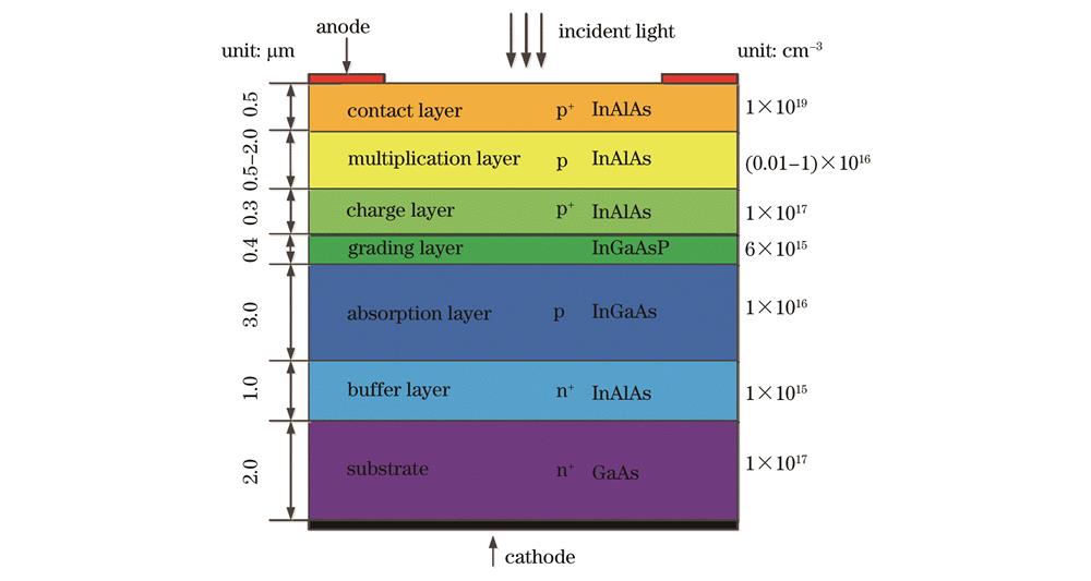
    Fig. 1. Schematic diagram of device structure
    Energy band and electric field distribution of device
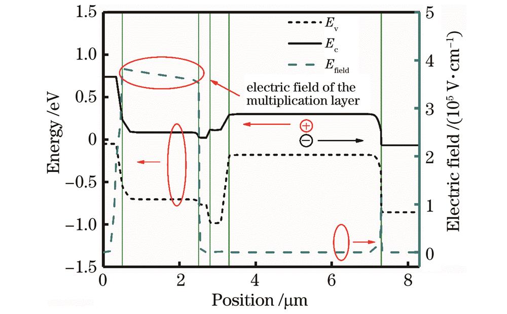
    Fig. 2. Energy band and electric field distribution of device
    Relationship between refractive index and wavelength. (a) InGaAs material; (b) InAlAs material
    Fig. 3. Relationship between refractive index and wavelength. (a) InGaAs material; (b) InAlAs material
    Current characteristics of device. (a) I-V characteristics; (b) gain
    Fig. 4. Current characteristics of device. (a) I-V characteristics; (b) gain
    Electric field distributions of device. (a) Effect of doping concentration of multiplication layer on electric field distribution;(b) effect of thickness of multiplication layer on electric field distribution
    Fig. 5. Electric field distributions of device. (a) Effect of doping concentration of multiplication layer on electric field distribution;(b) effect of thickness of multiplication layer on electric field distribution
    Effect of doping concentration of multiplication layer on Vp and Vb. (a) I-V characteristics; (b) change curves of Vp and Vb
    Fig. 6. Effect of doping concentration of multiplication layer on Vp and Vb. (a) I-V characteristics; (b) change curves of Vp and Vb
    Effect of thickness of multiplication layer on Vp and Vb. (a) I-V characteristics; (b) change curves of Vp and Vb
    Fig. 7. Effect of thickness of multiplication layer on Vp and Vb. (a) I-V characteristics; (b) change curves of Vp and Vb
    C-V characteristic of devices. (a) Effect of doping concentration of multiplication layer on capacitance; (b) effect of thickness of multiplication layer on capacitance
    Fig. 8. C-V characteristic of devices. (a) Effect of doping concentration of multiplication layer on capacitance; (b) effect of thickness of multiplication layer on capacitance
    ParameterInGaAsInAlAs
    Band gap /eV0.480.79
    Electron affinity /eV4.474.61
    Electron Shockley-Read-Hall(SRH)lifetime /s1×10-104×10-13
    Hole SRH lifetime /s1×10-104×10-13
    Electron mobility /(cm2·V-1·s-114482500
    Hole mobility /(cm2·V-1·s-1269233
    Electron Auger coefficient /(cm6·s-17×10-297×10-29
    Hole Auger coefficient /(cm6·s-17×10-297×10-29
    Effective conduction band density of states /cm-31.26×10172.61×1017
    Effective valence band density of states /cm-31.1×10197.63×1018
    Permittivity14.6313.96
    Table 1. Material parameters in simulation model
    Wei Ye, Pengfei Du, Beibei Quan, Mengfei Li, Sheng Xiao, Jia Liu. Effect of In0.83Al0.17As Multiplication Layer on Characteristics of In0.83Ga0.17As/GaAs Avalanche Photodetector[J]. Acta Optica Sinica, 2023, 43(4): 0404001
    Download Citation