
Yufei Xing, Jiaxing Dong, Sarvagya Dwivedi, Umar Khan, Wim Bogaerts. Accurate extraction of fabricated geometry using optical measurement[J]. Photonics Research, 2018, 6(11): 1008
- Photonics Research
- Vol. 6, Issue 11, 1008 (2018)
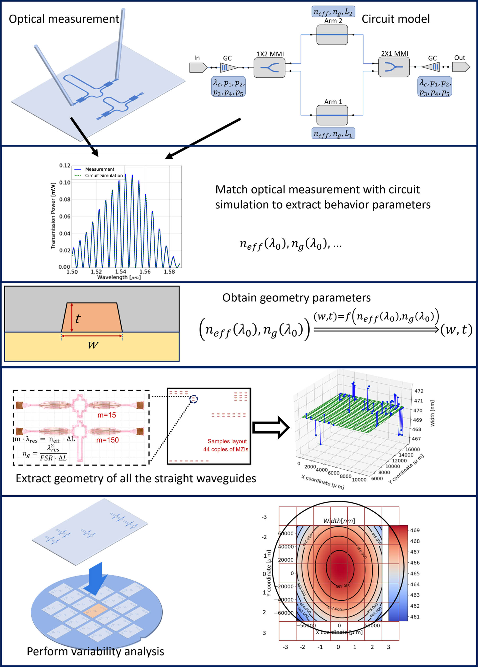
Fig. 1. Work flow of extracting behavior parameters and fabricated geometry using optical measurements.
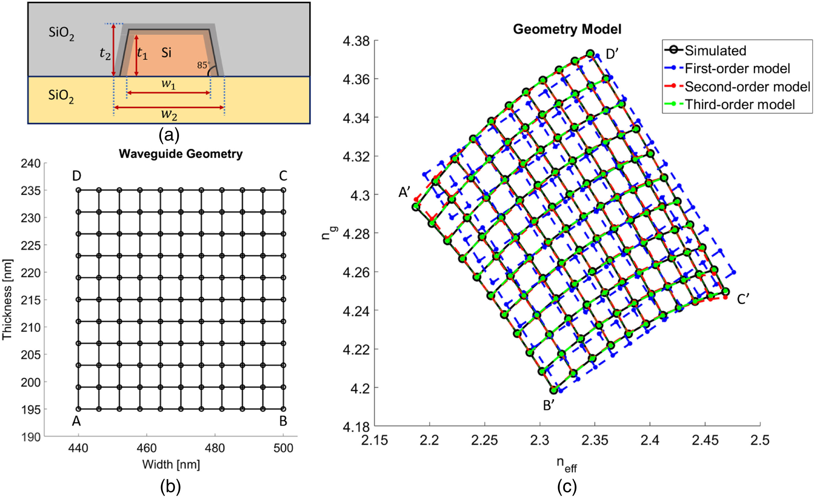
Fig. 2. (a) Cross-section schematic of an oxide-clad SOI strip waveguide with a 85° sidewall angle; (b) width and thickness grid of strip waveguides; (c) effective and group indices of strip waveguides on the geometry grid using the COMSOL FEM simulation, and the first-, the second-, or the third-order polynomial mapping model.
Fig. 3. Error contour plot of the proposed third-order polynomial model where w
Fig. 4. (a) Layout of the MZI under test. (b) Circuit schematic of the MZI.
Fig. 5. We removed the GC envelope using a reference GC near the DUT. Fabrication variation caused the measured spectrum after GC removal to be far from ideal (as shown by the spectrum simulated by the circuit model), as ideally the peaks in the spectrum should have the same amplitude. After GC removal, we fitted the measured spectrum with the circuit model (Fig. 4 ), not including the GC. Red solid curve, measured transmission spectrum after removing the GC envelope using a reference GC. Blue dotted curve, fitted spectrum using the circuit model. Left, the low-order MZI. Right, the high-order MZI.
Fig. 6. This figure shows the measured transmission spectrum (red solid curve) and fitted spectrum (blue dotted curve) using the circuit model including the polynomial GC model. Also, valleys of the spectrum (green cross) are found by the peak detection method. Left, the low-order MZI. Right, the high-order MZI.
Fig. 7. Bounds of the extraction. (a) The bound of width and thickness. (b) Rectangle bound [11] parallelogram, reduced bounds by linear transformation of geometry bounds. (c) Rectangle bounds cannot separate three groups of solutions (red, blue, and green circles). The parallelogram cleanly isolates the correct solutions (blue circles).
Fig. 8. Top left, low-order and high-order MZIs we used for geometry extraction. Bottom left, locations of two devices on a die. Right, locations of dies on the wafer. Red grid indicates dies on the wafer. The black circle is the boundary of the wafer.
Fig. 9. Extracted n eff n g X = 0 Y = 0 X = − 2 Y = 2
Fig. 10. x y X = 0 Y = 0 X = 0 Y = 0 X = − 2 Y = 2 X = − 2 Y = 2
Fig. 11. We extracted the linewidth and thickness on the same device over 21 dies on the wafer. Top left, systematic linewidth variation; bottom left, random linewidth variation; top right, systematic thickness variation; bottom right, random thickness variation.
|
Table 1. Error of Polynomial Models
|
Table 2. Comparison between the Peak Detection Method and the Curve Fitting Methoda
|
Table 3. Fitting Error versus Interference Order
| |||||||||||||||||||||||||
Table 4. Statistical Results for the Manufacturing Variations of a 200 mm Wafer Fabricated through a 193 nm DUV Lithography Process

Set citation alerts for the article
Please enter your email address
© Copyright 2018-2021 | Chinese Laser Press. All Rights Reserved 沪ICP备15018463号-20