Yufei Xing, Jiaxing Dong, Sarvagya Dwivedi, Umar Khan, Wim Bogaerts. Accurate extraction of fabricated geometry using optical measurement[J]. Photonics Research, 2018, 6(11): 1008
Copy Citation Text
We experimentally demonstrate extraction of silicon waveguide geometry with subnanometer accuracy using optical measurements. Effective and group indices of silicon-on-insulator (SOI) waveguides are extracted from the optical measurements. An accurate model linking the geometry of an SOI waveguide to its effective and group indices is used to extract the linewidths and thicknesses within respective errors of 0.37 and 0.26 nm on a die fabricated by IMEC multiproject wafer services. A detailed analysis of the setting of the bounds for the effective and group indices is presented to get the right extraction with improved accuracy.
1. INTRODUCTION
The submicron silicon-on-insulator (SOI) platform for silicon photonics offers tight confinement of light and compact integration of photonic devices. However, the high material index contrast also makes devices very sensitive to the geometry variation [1]. The variation introduced in fabrication often significantly deteriorates the device performance. Especially for spectral filters, geometry variation causes a shift in the spectrum and needs good compensation [2,3]. Therefore, an accurate evaluation of the fabricated geometry helps to estimate how to compensate the performance error and make a sensible design.
Extracting the fabricated linewidth and layer thickness is essential in getting the input data for analysis, such as performance evaluation [4,5] variability analysis [6,7], and revising compact behavior models [8]. However, metrology measurement of a fabricated photonic chip using a scanning electron microscope (SEM) is both expensive and destructive. Conventionally, the semiconductor fab only takes a few destructive cross-section pictures at given wafer locations on different dies, and this is only during process development, not in production. The geometry accuracy of such SEM-based measurements is usually good for a qualitative confirmation but not accurate enough for exact modeling. Ultraprecise methods such as the atomic force microscope (AFM) are extremely time-consuming [9]. In production, nondestructive methods such as top-down SEM, ellipsometry, and scatterometry are used to measure geometries such as linewidth and layer thickness. The problem with such measurements is that they are collected in dedicated measurement sites, which are often not representative of the actual waveguide devices. Current methods are not capable of extracting accurate wafer maps of the actual device geometry on a nanometer scale and its variability.
An alternative approach is to use optical transmission measurements on the actual devices to extract geometry parameters. Investigating the spectral response of devices such as microdisks or long Bragg gratings offers a more efficient way of characterizing manufacturing variations. However, most demonstrated methods either use dual-polarization measurements or request complex spectral reflection measurements from both ends of the device [4,10]. Optical properties such as the effective index and group index can be extracted from interfering structures such as Mach–Zehnder interferometers (MZIs) [11] and ring resonators [5,12]. Recent research shows the possibility to correlate waveguide geometry with these behavioral parameters such as resonance wavelength and group index by mapping them with a linear model [5]. Lu et al. measured spectral responses of ring resonators over the wafer and from this derived a geometry wafer map, demonstrating the potential of the optical method for wafer-scale geometry extraction. In this study, they used a ring resonator that consists of both straight and bent waveguides. Since straight and bent waveguides have different effective and group indices, the geometrical cross section of a straight waveguide cannot be extracted accurately from a ring, without making assumptions on the straight and bent geometry that cannot be verified.
Sign up for Photonics Research TOC. Get the latest issue of Photonics Research delivered right to you!Sign up now
Even though geometry extraction through transmission measurements shows real practical potential, it is still challenging to characterize the manufacturing quality accurately. First of all, the geometry model that links geometry with the behavior parameters should on one hand be very accurate, but on the other hand have as few parameters as possible. This is hard to achieve with combinations of different waveguide types (straight and bent), each with their own optical properties. Second, there is always noise in the spectral measurements, error in measurement alignment, and variability in grating couplers (GCs). It is essential to develop a method that is tolerant of the above-mentioned factors. Third, geometry extraction requires a method to simultaneously extract both effective and group indices from the same device. Most importantly, it is not trivial to get the correct effective index from the spectrum of an interfering device [13]. We need a quantitative discussion to choose the right effective index from many possible solutions.
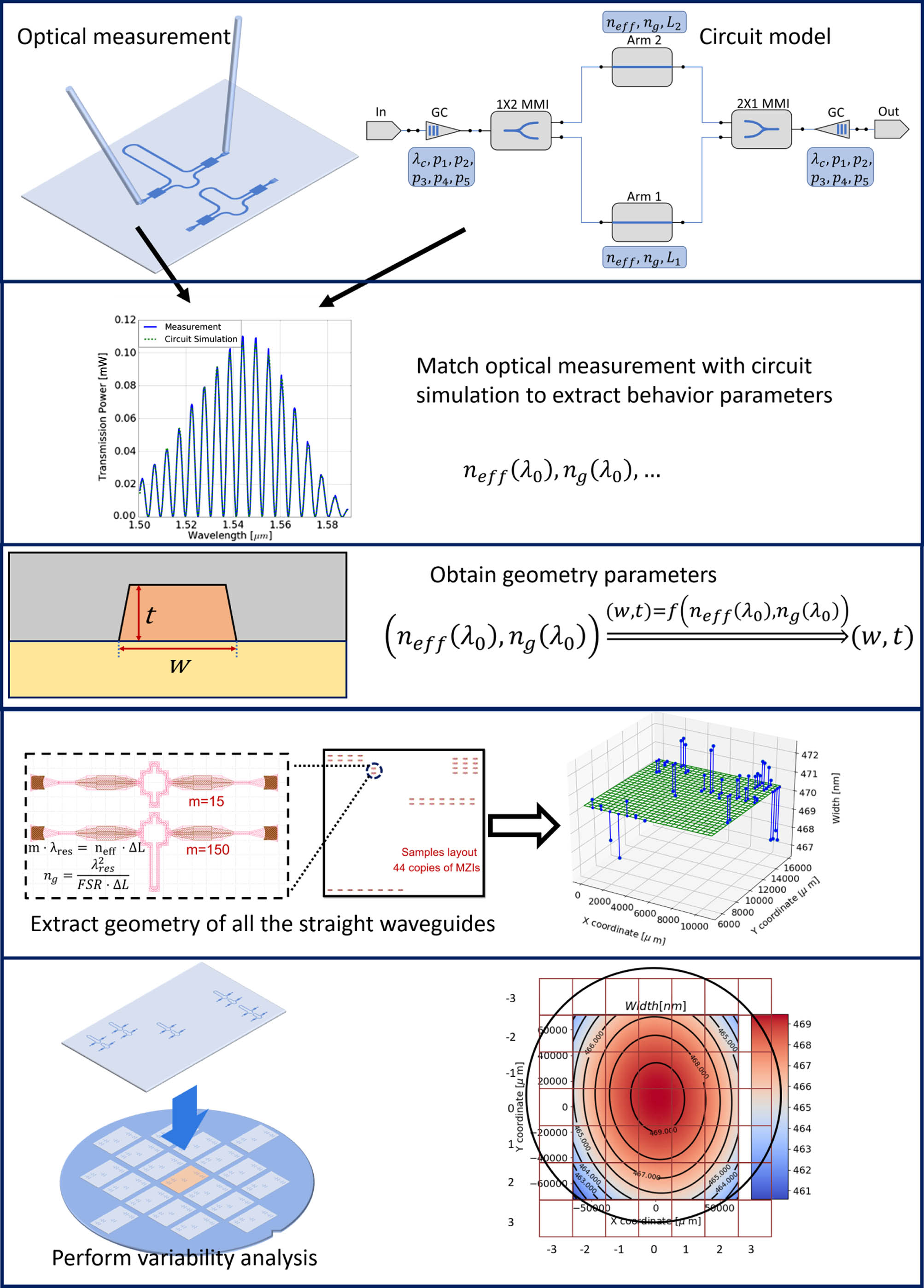
In this paper, we address the above-mentioned challenges in a systematic way. As shown in Fig. 1, we first perform optical measurements on MZIs. We build a circuit model of the device and match the simulated transmission curve with measurement to get behavior parameters of a waveguide such as and . Next, we build an accurate model to map and to waveguide width and thickness. Then, using the model, we obtain waveguide geometry parameters from extracted behavior parameters. We automated the optical measurement and repeated the geometry extraction on devices with the same design over the wafer. From the extraction, we perform variability analysis and derive fabrication variation with high accuracy. In Section 2, we propose an improved geometry model to offer high modeling accuracy. In Section 3, we show that the curve fitting method is less sensitive to measurement noise and helps in removing GC envelope, and in Section 4, we show how to design two MZIs to extract the accurate and unique and given the waveguide geometry variation range. Section 5 discusses the procedure of the waveguide geometry from a couple of MZIs. Finally, in Section 6, we apply the method to extract linewidths and thicknesses of SOI waveguides on a die fabricated by the IMEC multiproject wafer (MPW) service.
Figure 1.Work flow of extracting behavior parameters and fabricated geometry using optical measurements.
We cannot measure linewidth and thickness directly, so we infer them from the results of optical transmission measurements. In particular, we first extract the effective index and group index of the waveguide. To calculate the fabricated waveguide linewidth and thickness from the effective index and group index , we require a geometry model that links and to and . To build the model, we simulated an oxide-clad Si waveguide cross section [Fig. 2(a)] with the COMSOL Multiphysics finite element method (FEM) solver. According to the IMEC technology handbook, a fabricated strip waveguide has a sidewall angle of 85°, so we simulated the waveguide with an 85° sidewall angle. The waveguide width is the bottom width of the trapezoid. We swept width from 440 nm to 500 nm and thickness from 195 nm to 235 nm, and calculated and at 1550 nm wavelength. The linewidth-thickness grid in Fig. 2(b) can be mapped one-on-one to the simulated – grid (black solid line with circles) in Fig. 2(c). Then, we fitted simulated and using polynomials of and . We build first-, second-, and third-order polynomial models [dashed lines in Fig. 2(c)]. Both and vary quite linearly with and . Nonetheless, the first-order fitted linear model shows a clear deviation (maximum 0.32% error in and 0.40% in ) from simulated and . The third-order model matches the simulation very accurately. Then, to get and from spectral measurements, we wrote and , as a polynomial of and at 1550 nm as where and are constant terms, and and are coefficients in polynomials.
Figure 2.(a) Cross-section schematic of an oxide-clad SOI strip waveguide with a 85° sidewall angle; (b) width and thickness grid of strip waveguides; (c) effective and group indices of strip waveguides on the geometry grid using the COMSOL FEM simulation, and the first-, the second-, or the third-order polynomial mapping model.
Using a simulated model can introduce a simulation error, coming from a difference between the actual waveguide geometry (both dimensions, shape, and material properties) and the trapezoidal geometry model we used in the mode solver. We have considered the sidewall angle in our model, but still we do not know the actual geometry, so it is very hard to compensate for this error. This means that some parameters will be only relative. In addition, the mapping error is the difference between the simulated trapezoidal waveguide geometry and extracted trapezoidal waveguide geometry using the geometry model. To calculate the mapping error, we first use simulated and for simulated geometry. Then, we calculate the waveguide geometry using a polynomial model with the simulated and . The mapping error reduces significantly with the order of the polynomial (Table 1). The first-order model has a maximum error of several nanometers, which is comparable to the reported intra-wafer manufacturing variations in width of 0.78 to 2.65 nm, and in thickness of 0.83 to 4.16 nm [14–19]. Obviously, the modeling error is too large to extract intra-die variations (variations between the same devices on one die). For a good estimation of the fabricated geometry variation, especially to study variability on the intra-wafer level and the intra-die level, a lower modeling error is required. The third-order polynomial model has a maximum error of 0.05 nm for both linewidth and thickness (Fig. 3), which is one magnitude smaller than the fabrication variation. A low modeling error makes geometry extraction more accurate and credible.
Figure 3.Error contour plot of the proposed third-order polynomial model where ranges from 440 to 500 nm and thickness ranges from 195 to 235 nm. Left, width extraction error; right, thickness extraction error.
3. EXTRACTING neff AND ng FROM AN MZI USING THE CURVE FITTING METHOD
Before we can determine the waveguide geometry from and , we need to measure those quantities on a device and isolate the values for a straight waveguide. This effectively means that we need a device where a transmission measurement can give us an accurate extraction of both and of a straight waveguide only, and which is in the presence of measurement noise and variation in the coupling structures.
In Ref. [5], ring resonators were used to extract and . A ring resonator has sharp resonance peaks that are easy to detect and less prone to error in peak positions. However, a ring uses either a bent waveguide or it combines bends with straight sections, and the round trip path also includes the coupling sections, which will also have different optical properties. As such, we cannot isolate and of the straight or bent waveguide. The alternative is to use an MZI with two arms that are identical except for that one arm has a longer straight part than another [11]. Ideally, the and of the two arms are identical so that the spectral response of the MZI is only dependent on the path length difference between two arms. We can use MZI to measure varying waveguide geometry under process variation at different locations. In practice, the path length difference in a single MZI is also induced by a difference in in the two arms because of process variability. Also, there is also the difference in that the bends will contribute to. Those differences also lead to the extraction error in and . However, since the distance between waveguides within an MZI compact is within 100 μm, we can safely assume that the error will be much smaller than the device-to-device variation.
An interfering structure such as a ring or an MZI would have a constructive interference when interference order is an integer and where is the prior estimate at the resonance wavelength and is the physical path length difference. If we know the resonance order , we could get by locating in the output spectrum. It is natural to apply the resonance detection method [5,12] to locate resonances in the spectrum and get both and . However, an MZI has a sinusoidal-like spectral transmission. Its curve is quite flat near a maximum or minimum. Especially when measurement noise is involved, it is hard to locate its resonance by the peak detection method (in Fig. 6, the green cross indicates detected valleys). Using only the maximum detection method leads to a significant error (Table 2) in effective index and group index extraction, making it not suitable for geometry extraction.
neff
ng
Width [nm]
Thickness [nm]
Curve fitting using a GC model
2.319
4.291
466.0
211.8
Peak detection
2.318
4.302
462.0
213.8
Difference between two methods
0.001
0.009
4.0
2.0
Table 2. Comparison between the Peak Detection Method and the Curve Fitting Methoda
To improve the extraction accuracy, we used the curve fitting technique. It extracts parameters by minimizing the difference between a circuit simulation and the measurement data. While maximum/minimum extraction only uses information at the peaks and ignores information on the rest of the spectrum, the curve fitting method utilizes the information from the entire measured spectrum, which is more tolerant to the measurement noise and gives more reliable extraction.
We simulate the MZI circuit in Caphe [20], a circuit simulator that calculates the scattering matrix of the circuit from the defined scattering matrix of each component. We built a Caphe circuit model of the MZI in the same way as our device under test (DUT), which has two types of components: waveguide and multimode interferometer (MMI).
A. Eliminating the Effect of the Grating Couplers
For automated measurement, light is vertically coupled to the DUT using a pair of GCs. We need to remove the envelope of the GC before fitting the spectrum with the circuit model. We can remove the GC in two ways. In one way, we measure a pair of reference GCs, preferably close to the DUT. By subtracting the measured reference GC from the DUT spectrum in a log scale, we can normalize the transmission spectrum of the DUT. It is a very common practice in optical transmission measurements. However, this method is error-prone in the presence of fabrication variation in GCs, because the reference GC can be subtly different from the GCs connected to the DUT. Even more, the input and output GCs of the DUT can be different from each other. As shown in Fig. 5, MZI transmission after subtracting the reference is not we would expect: the linear-scale spectrum should be a sine-like curve with maxima of the same amplitude. The significant mismatch between the measured and fitted spectrum introduces a large error in the extracted parameters.
Figure 4.(a) Layout of the MZI under test. (b) Circuit schematic of the MZI.
Figure 5.We removed the GC envelope using a reference GC near the DUT. Fabrication variation caused the measured spectrum after GC removal to be far from ideal (as shown by the spectrum simulated by the circuit model), as ideally the peaks in the spectrum should have the same amplitude. After GC removal, we fitted the measured spectrum with the circuit model (Fig. 4), not including the GC. Red solid curve, measured transmission spectrum after removing the GC envelope using a reference GC. Blue dotted curve, fitted spectrum using the circuit model. Left, the low-order MZI. Right, the high-order MZI.
Figure 6.This figure shows the measured transmission spectrum (red solid curve) and fitted spectrum (blue dotted curve) using the circuit model including the polynomial GC model. Also, valleys of the spectrum (green cross) are found by the peak detection method. Left, the low-order MZI. Right, the high-order MZI.
Instead, we use a fourth-order polynomial to represent the logarithmic transmission spectrum of the combined input and output GC. We include two GCs in the circuit model together with the MZI. As shown in Fig. 6, the fitting is considerably enhanced where the simulation matches measurement nicely. From fitting, we can get circuit parameters such as effective index, group index, and coefficients of the polynomial describing the GC.
B. Fitting Accuracy versus MZI Order
In the transmission spectrum of the MZI, the positions of the peaks and valleys give information about the effective index . The periodicity of the transmission spectrum is determined by the group index . An MZI with a low-order has only a few peaks/valleys in the measurement band, and therefore it will have a low accuracy on the extraction of . On the other hand, a high-order MZI can give a high accuracy of extraction. As explained by Dwivedi et al. in Ref. [11], the combination of a low-order MZI and a high-order MZI can give a good accuracy on both and . When noise is mingled in the measured spectrum, it will induce in curve fitting an error. Then, it is a question of how fitting accuracy is related to the order of the MZI. In this work, we used the nonlinear least squares method to fit the transmission curves with a waveguide compact model. We built a circuit model of a waveguide with 470 nm width and 215 nm thickness and simulated the transmission spectrum. Then, we add a to the spectrum to emulate the typical measurement noise. Finally, we get and using the curve fitting. The fitting error we presented is the estimate of 1.96 times standard deviations of each of the parameters, which provides confidence limits of approximately 95%. As shown in Table 3, we did not get an accurate from the 15-order MZI. This leads to a huge error in extracted width and thickness. The fitting error decreases with the interference order. Therefore, an increasing interference order of the MZI improves fitting accuracy.
When fitting the transmission curve of the MZI, the fitting algorithm implicitly assumes that the order of the MZI is sufficiently accurate, i.e., that the peak near the center wavelength of 1550 nm corresponds with the designed order . However, in the presence of fabrication variation, this is not necessarily the case, and as the designed order of the MZI increases, the uncertainty on the measured order increases. Therefore, the design parameters should be chosen such that the low-order MZI can be used to pin the order of the device unambiguously [11], and make a good estimate of . The order of the high-order MZI should be chosen such that a maximum of information can be extracted, based on the estimate of obtained from the low-order MZI. We discuss the design process for these devices.
A. Deciding the Interference Order under a Given neff Variation
Equation (4) shows that if we know the resonance order , we can calculate from the peak locating in the output spectrum. However, if fabrication variations can shift the spectrum more than half a free spectral range (FSR), we can no longer be certain of the order . Therefore, we should design the MZI with sufficiently low-order such that the order at the center wavelength is always within , which means Given the variation in is , we can decide the order that fulfills the condition and would give us sufficient confidence: This is equivalent to a constraint on the length difference between the two arms of the MZI:
B. Defining the Bounds for neff and ng from the Geometry Variation
Within the measurement interval, the spectrum of an MZI looks quasi-identical if we shift the interference order by an integer number. Without a proper confidence interval on , there would be multiple solutions of to fit the spectrum. As and can be mapped to linewidth and thickness , we can derive the bound of from the confident interval of the geometry parameters , which are supplied by the fab. As presented in Section 2, and can be accurately mapped on and by a third-order polynomial model. For simplicity of analysis in the derivation below, we use the linear geometry model, where When the bounds for linewidth and thickness form the rectangle in space [Fig. 7(a)], the parameter range in space lies in between and : where and are the nominal values for and variations. The range is a rectangle in space whose center is . We assume and . As and follow a near-linear mapping, the vertices of the bound rectangle in the space , , , can be mapped to the space as , , , . Intuitively, the bound rectangle in space is linearly transformed into a parallelogram in space. The tilted boundary is within the original rectangular boundary and much smaller. For the fundamental TE mode of an SOI oxide-clad waveguide, is negative while , , and are positive. The parallelogram then will be tilted as in Fig. 7(b).
Figure 7.Bounds of the extraction. (a) The bound of width and thickness. (b) Rectangle bound [11] parallelogram, reduced bounds by linear transformation of geometry bounds. (c) Rectangle bounds cannot separate three groups of solutions (red, blue, and green circles). The parallelogram cleanly isolates the correct solutions (blue circles).
The bounds of the confidence interval for are fundamental to get a correct extraction. Extraction of the group index does not pose that much of a problem, as the confidence interval is much larger, and there are no multiple solutions. Depending on whether we know of the same waveguide, we can estimate the range for in two ways.
1. Estimating neff without Information on ng
Sometimes we cannot obtain accurate information of , such as when we are using a low-order MZI. Then, as in Ref. [11], we can calculate the uncertainty from geometry variations and as which essentially corresponds to the width of the rectangle , or the horizontal distance .
2. Estimating neff with Information on ng
The maximal range of the for a given is [Fig. 7(b)], which is the maximal distance between two edges of the parallelogram at the given . The distance is dependent on the shape of the parallelogram. When is higher than [], using Eq. (7), we can derive . Then, is the horizontal distance between lines and , and the range of is determined by the range of linewidth . When is lower than [], using Eq. (7), we can derive . Then, is the horizontal distance between lines and , and the range of is determined by the range of thickness : For the same geometry variation, an estimate of reduces the uncertainty . Figure 7(c) shows that we can separate three groups of solutions with the bound , which are all located in the previous rectangle bound. Also, becomes solely dependent on in the linear approximation. So if we have a small and a relatively large , we can benefit more from knowing , because we can use a high-order MZI that improves the accuracy of extraction. When , the ratio between calculated without and with is where Both and are positive, so that the ratio is increasing with . Intuitively, the smaller that is compared to in Fig. 7(a), the shorter the is. A similar conclusion can be made when , where the ratio is increasing with .
5. EXTRACTION PROCEDURE
A. Extracting neff and ng from Two MZIs
The total process variation (intra-die, die-to-die, and wafer-to-wafer) on an isolated waveguide on an SOI platform is large. The variation can be several tens of nanometers for both linewidth and thickness. As discussed in the previous section, to capture the large variation using an MZI, we should choose a sufficiently low-order . However, this low-order MZI suffers from a low accuracy on extraction. On the other hand, a high-order MZI can offer good accuracy of extraction. So a combination of the two devices can give us both essential optical parameters. So we can extract and using a low-order MZI and a high-order MZI:
Extract a good estimate of from the low-order MZI.
Extract an accurate from the high-order MZI.
Even though the devices are close together, they do not have the same and because of local variations. To accurately map the waveguide geometry, we need to extract both and from the same waveguide. In the following discussion, we will present how to obtain an accurate and both of the high-order MZI step by step.
B. Extracting Inter-Die and Intra-Die Variability in Three Steps
In a wafer-scale fabrication process, we can identify different levels of process variations. For each die, all the variations that originate at levels such as lot-to-lot, wafer-to-wafer, and die-to-die variations have the same impact on every device in the die. In this paper, we categorize these variations together as the inter-die variation. However, then we also get the intra-die variation that affects devices differently on the same die. We can further decompose the intra-die variation into location-dependent variation and local variation. The location-dependent variation is the variation depending on the location of the device on the die. It can be caused by the continuous variation of thickness, photoresist spinning effects or plasma distributions, and other equipment nonuniformity that affects the fabricated geometry varied spatially. On the other hand, the local variation we define here induces local disparities between devices placed close together (less than a few hundred microns apart). It includes intrinsic variability such as thickness fluctuations and width randomness caused by pattern density nonuniformity. The sum of the three variations gives us the process variation of a device: The total process variation is considerably larger than the intra-die variability. The total linewidth and thickness variation of an isolated waveguide on an SOI platform can amount to tens of nanometers [15], while intra-die variation is typically only a few nanometers [5,15,16,21].
With our two MZIs, we address variations on the different levels in three steps. In the first step, we extract from a low-order MZI. Since the extracted from the low-order MZI is very inaccurate, we estimate the range of without the information of by substituting geometry variation by the total variation in Eq. (11): Given the range, we derive a fairly accurate value of from the low-order MZI. In the second step, we obtain the map over the die by interpolation. The map offers the average of the waveguide placed at each location where we can remove the local variation, and the inter-die variation and location-dependent variation together determine the average value. In the third step, we use interpolated at each location as a reference. Now, rather than the total variation, we can only deal with the much smaller local variation. Since we can accurately extract on the high-order MZI, the range for under the local variation is estimated by substituting geometry variation using the local variation in Eq. (12): Because our analysis decreases the bound of extraction, we can use a much high-order MZI to get and simultaneously and accurately.
C. Specification of the Two MZIs
The MZIs each consists of two waveguide arms and two 50-50 MMIs (Fig. 8 left). Our devices are fabricated by the IMEC MPW service. We design the waveguide with a linewidth of 450 nm. According to the technology handbook, the fabricated waveguide has a sidewall angle of 85°. The fabricated 450 nm waveguide will have a 470 nm mean value and variations. The nominal thickness is 215 nm, and the variation is . The pre-estimated of the waveguide is 2.340. Using Eq. (11), we calculated that the variation of is From the third-order model, we calculate that the is also 0.16. The arm length difference of the low-order MZI is , and the order of .
Figure 8.Top left, low-order and high-order MZIs we used for geometry extraction. Bottom left, locations of two devices on a die. Right, locations of dies on the wafer. Red grid indicates dies on the wafer. The black circle is the boundary of the wafer.
Only a few references report typical fabricated geometry maps of silicon waveguides on die-level. Thickness maps in SOI depend largely on the qualities of the source wafer. Linewidth maps depend much more on the actual fabrication process and will be very different for devices fabricated with deep UV lithography or e-beam lithography, and vary between fabs. From the research of Lu et al.[5], the thickness varies slowly over the die, and the maximum difference between neighboring thickness is 0.5 nm. So we assume as a worst case that the thickness is slowly changing locally with only . We also assume that , which is significant. Using Eq. (12), we calculated the variation of . Notice that we have no pre-estimate of the nominal value of and locally so that they can be any value under the total variation. We calculated for and . Its value is in between 0.0045 and 0.0074. Therefore, the max local variation we can surely extract is which is the same calculated using the third-order model. The arm length difference of the high-order MZI is , where the order is around . The confidence limit estimated with the information on on the order is that calculated by the original method without the information on . Based on the estimation, we design the low-order MZI to have an order around at 1550 nm and the order of the high-order MZI is .
6. RESULTS
We automated optical measurements on 21 dies in the same wafer. The optical measurement was conducted in our clean room with the room temperature controlled at 20°C. On each die, we distributed 44 copies of the MZI pair (Fig. 8, bottom left) and repeated the fitting for all MZI blocks. With the estimated process variations on different levels, we set up the bound for and followed the three-step procedure to extract and of high-order MZIs (Fig. 6, right). Each point in the scatter plot represents the extracted and of one waveguide on the die (Fig. 9). All the points are gathered in one group as confined by the bound. The average fitting error for is , and the average fitting error for is . These fitting errors propagate to fitting errors of 0.33 nm in width and 0.18 nm in thickness. Adding the mapping error of the geometry model in Section 2, the total extraction errors for width and thickness are Using the geometry model, we mapped and to width and thickness of the high-order MZI arms. The extracted linewidth on the die (, ) in the wafer center (Fig. 8, right) ranges from 468.8 nm to 471.9 nm, and the thickness ranges from 211.4 nm to 212.3 nm. The standard deviations are 1.26 nm and 0.30 nm, respectively (Table 4). The extracted linewidth on the die (, ) near the boundary of the wafer ranges from 461.4 nm to 466.8 nm, and the thickness ranges from 212.1 nm to 214.0 nm. The standard deviations are 1.18 nm and 0.42 nm, respectively (Table 4). For both dies, we observed a very weak correlation (correlation coefficient is ) between the linewidth and the thickness. We fitted width and thickness to its location on the die with a linear model, and the green grid is the fitted map (Fig. 10) that indicates the location-dependent variation. We did observe a systematic trend for width on this die, but the trend is quite flat on each die, which is less than 1 nm. Meanwhile, the width shows an obvious local variation with a maximum of 3 nm. For thickness , both dies exhibit location dependency, which might be the result of slow-varying systematic variation over the wafer. Local variation has a maximum of 0.5 nm, well below the local variation range we set in the extraction. The maximum location-dependent difference in thickness on the die (, ) is 0.4 nm while on the die (, ) is 1.5 nm.
Figure 10. and coordinates give the locations of the MZIs on two dies. Blue solid dot, extracted value. Green grid, fitted map of extracted values using a bivariate polynomial. (a) Extracted width map of die (, ) (in the center of the wafer). (b) Extracted thickness map of die (, ). (c) Extracted width map of die (, ) (near the edge of the wafer). (d) Extracted thickness map of die (, ).
We also extracted a width and thickness wafer map of one pair of MZIs that share the same location on every die. The extracted wafer map (Fig. 11) shows an explicit location dependence of fabricated geometry. We fit a parameter wafer map of , using a second-order bivariate polynomial. The slow-varying trend of the linewidth matches the dome-like radial symmetric pattern of the wafer-level systematic variation. The width systematic variation ranges from 459 nm to 465 nm while the random part has a maximum 2 nm contribution. The thickness also presents a strong location dependence. Its systematic variation ranges from 211.5 nm to 214.5 nm. Its random variation has a maximum of less than 1 nm.
Figure 11.We extracted the linewidth and thickness on the same device over 21 dies on the wafer. Top left, systematic linewidth variation; bottom left, random linewidth variation; top right, systematic thickness variation; bottom right, random thickness variation.
We show how to extract waveguide geometry from optical transmission measurement, and discuss how to increase the accuracy compared to existing methods. We replaced the linear mapping model between and with an accurate third-order geometry model to obtain accurate waveguide geometry from its effective index and group index. We applied a curve fitting method that is less sensitive to measurement noise and helps in removing the GC envelope. We discussed how to set parameter bounds under a given process variation, which helps to choose the correct set of extracted parameter values from multiple solutions. We showed that, when the group index of a waveguide is known, we can reduce the parameter bounds for the effective index, allowing us to use a higher order MZI and improve fitting accuracy. We proposed a procedure to separate different levels of process variation so that our method can deal with a total variation of several tens of nanometers and still obtain accurate linewidth and thickness extraction. We applied the method to measurement data from two dies and presented the linewidth and thickness map on die-level. We also applied the method to extract one pair of MZIs in 21 dies and presented a simple wafer map of fabricated geometry.
Acknowledgment
Acknowledgment. Part of this work is supported by the Flemish Research Foundation (FWO-Vlaanderen) and by the Flemish Agency for Innovation and Entrepreneurship (VLAIO) with the MEPIC project.
APPENDIX A: PROCEDURE TO APPLY THE CURVE FITTING M
Calibrate the laser before the measurement to assure the wavelength accuracy of the measurement spectrum.
Calibrate the laser after the entire measurement to assure the stability of the laser.
Measure a reference pair of GCs. Fit its log-scale transmission with a four-order polynomial. Use the fitted coefficients of the polynomial as the nominal values for GC parameters in the circuit model.
Use the circuit model of the MZI and the curve fitting method to extract from the low-order MZI. Estimate the bound of from the total fabrication variation on the waveguide linewidth and thickness. Since we have no accurate knowledge of of the low-order MZI, set the bound of using Section 4.B.1.
Extract of the low-order MZI over the die. Fit the die map using first-order/second-order polynomials.
Use the circuit model of the MZI and the curve fitting method to extract and from the high-order MZI. Estimate the nominal value of at each die location using the fitted die map from low-order MZIs. Estimate the bound of from intra-die fabrication variation on the waveguide linewidth and thickness. Since we can extract accurately from the high-order MZI, set the bound of using Section 4.B.2.
Extract and of the high-order MZI over the die.
Map and to linewidth and thickness using the third-order geometry model.
Plot the die map of width and thickness. Identify obvious outliers in the thickness map and check the errors of the corresponding curve fitting to evaluate the problem.
[2] A. Ribeiro, S. Dwivedi, W. Bogaerts. A thermally tunable but athermal silicon MZI filter. 18th European Conference on Integrated Optics 2016 (ECIO)(2016).
[12] T. Horikawa, D. Shimura, H. Takahashi, J. Ushida, Y. Sobu, A. Shiina, M. Tokushima, S.-H. Jeong, K. Kinoshita, T. Mogami. Extraction of SOI thickness deviation based on resonant wavelength analysis for silicon photonics devices. IEEE SOI-3D-Subthreshold Microelectronics Technology Unified Conference (S3S), 10, 1-3(2017).
[15] S. K. Selvaraja, E. Rosseel, L. Fernandez, M. Tabat, W. Bogaerts, J. Hautala, P. Absil. SOI thickness uniformity improvement using corrective etching for silicon nano-photonic device. IEEE International Conference on Group IV Photonics GFP, 71-73(2011).
[16] S. K. Selvaraja. Wafer-Scale Fabrication Technology for Silicon Photonic Integrated Circuits(2011).
[20] M. Fiers, T. Van Vaerenbergh, J. Dambre, P. Bienstman. CAPHE: time-domain and frequency-domain modeling of nonlinear optical components. Advanced Photonics Congress, IM2B.3(2012).
Yufei Xing, Jiaxing Dong, Sarvagya Dwivedi, Umar Khan, Wim Bogaerts. Accurate extraction of fabricated geometry using optical measurement[J]. Photonics Research, 2018, 6(11): 1008