• Journal of Semiconductors
  • Vol. 42, Issue 11, 112802 (2021)
Xi Wang1、2, Yiwen Zhong1, Hongbin Pu1、2, Jichao Hu1、2, Xianfeng Feng1、2, and Guowen Yang3
Author Affiliations
  • 1Department of Electronic Engineering, Xi'an University of Technology, Xi'an 710048, China
  • 2Xi’an Key Laboratory of power Electronic Devices and High Efficiency Power Conversion, Xi’an 710048, China
  • 3Sanli Intelligent Electric Co., Ltd, Xi’an 712000, China
  • show less
    DOI: 10.1088/1674-4926/42/11/112802 Cite this Article
    Xi Wang, Yiwen Zhong, Hongbin Pu, Jichao Hu, Xianfeng Feng, Guowen Yang. Investigation of lateral spreading current in the 4H-SiC Schottky barrier diode chip[J]. Journal of Semiconductors, 2021, 42(11): 112802 Copy Citation Text show less
    (Color online) Schematics of the device structures used in the simulation. (a) Considering the lateral spreading current. (b) Ignoring the lateral spreading current.
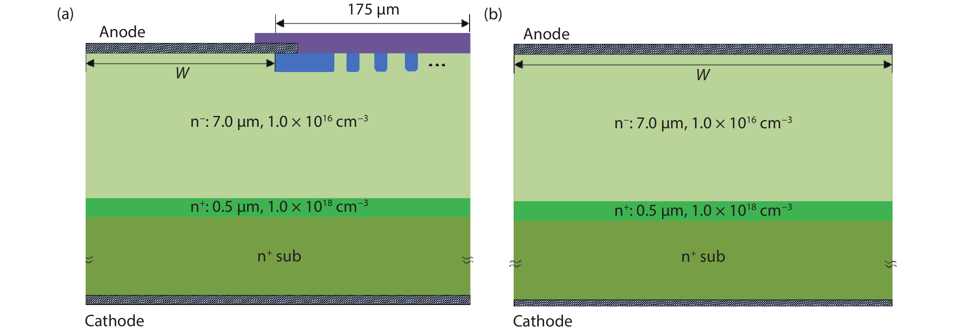
    Fig. 1. (Color online) Schematics of the device structures used in the simulation. (a) Considering the lateral spreading current. (b) Ignoring the lateral spreading current.
    Simulated relationship between chip size and proportion of spread current in the total forward current.
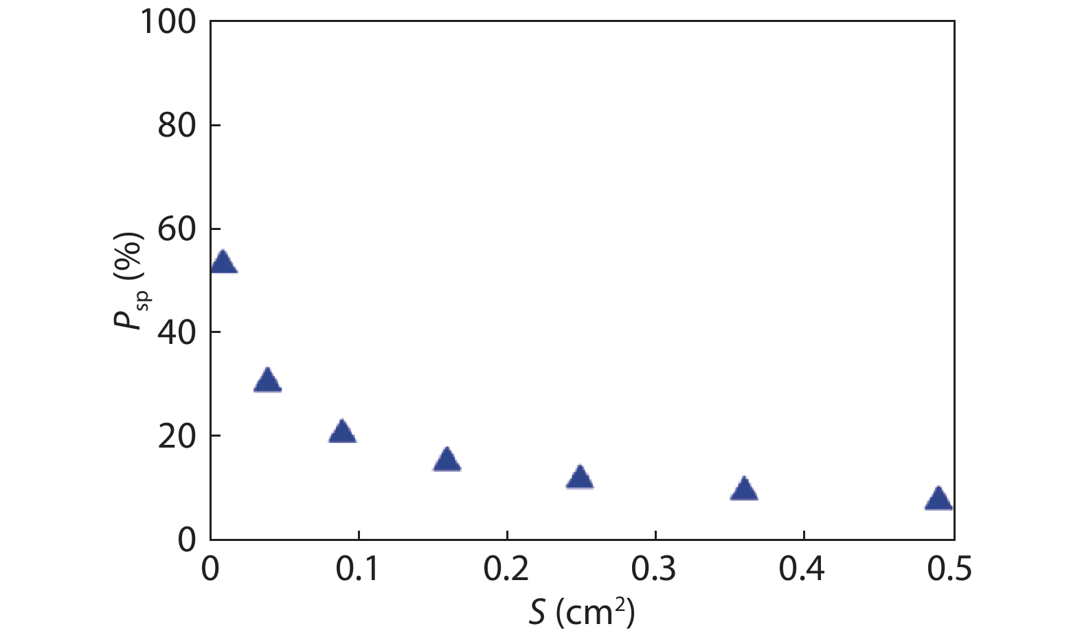
    Fig. 2. Simulated relationship between chip size and proportion of spread current in the total forward current.
    (Color online) Top view of the fabricated SiC SBD chip.
    Fig. 3. (Color online) Top view of the fabricated SiC SBD chip.
    (Color online) Current–voltage curves of the fabricated SBD chips. (a) Forward current–voltage curves. (b) Reverse current–voltage curves.
    Fig. 4. (Color online) Current–voltage curves of the fabricated SBD chips. (a) Forward current–voltage curves. (b) Reverse current–voltage curves.
    (Color online) Current density–voltage curves of the fabricated SBD chips. (a) Forward current density–voltage curves. (b) IF/SA–voltage curves. (c) Reverse current density–voltage curves. (d) IR/SA–voltage curves.
    Fig. 5. (Color online) Current density–voltage curves of the fabricated SBD chips. (a) Forward current density–voltage curves. (b) IF/SA–voltage curves. (c) Reverse current density–voltage curves. (d) IR/SA–voltage curves.
    (Color online) Schematic diagrams of the lateral current spreading in the 4H-SiC SBD chip. (a) Cross-section view. (b) Vertical view.
    Fig. 6. (Color online) Schematic diagrams of the lateral current spreading in the 4H-SiC SBD chip. (a) Cross-section view. (b) Vertical view.
    (Color online) Calculated Jsp and Psp at different anode voltages of the SBD chips.
    Fig. 7. (Color online) Calculated Jsp and Psp at different anode voltages of the SBD chips.
    Ksp–S curve and Psp of the fabricated SBD chips.
    Fig. 8. KspS curve and Psp of the fabricated SBD chips.
    ModelParameter
    Bandgap energy model[17]
    Incomplete ionization model[18]
    Mobility model[19]
    Impact ionization model[20]
    Schottky contact model[21]
    Table 1. Models and parameters used in the simulation.
    Xi Wang, Yiwen Zhong, Hongbin Pu, Jichao Hu, Xianfeng Feng, Guowen Yang. Investigation of lateral spreading current in the 4H-SiC Schottky barrier diode chip[J]. Journal of Semiconductors, 2021, 42(11): 112802
    Download Citation