
Xi Wang, Yiwen Zhong, Hongbin Pu, Jichao Hu, Xianfeng Feng, Guowen Yang. Investigation of lateral spreading current in the 4H-SiC Schottky barrier diode chip[J]. Journal of Semiconductors, 2021, 42(11): 112802
- Journal of Semiconductors
- Vol. 42, Issue 11, 112802 (2021)
Abstract
1. Introduction
Silicon carbide (SiC) has proved to be one of the most promising wide band gap semiconductor materials for high power electronic devices[
To reduce costs, the area of the 4H-SiC SBD chip has been scaled down by minimizing the resistance of the active area and narrowing down the length of the terminal[
In this paper, 4H-SiC SBD chips with a field limiting ring (FLR) terminal are simulated and fabricated. The lateral current spreading in the 4H-SiC SBD chip is investigated and calculated. Moreover, the effect of the lateral current spreading on the forward performance of the device is discussed and analyzed.
2. Simulation
To investigate the lateral spreading current in the 4H-SiC SBDs, simulations are carried out using Silvaco TCAD tools. Table 1 lists the physical models and the parameters, including the bandgap energy model[
![]()
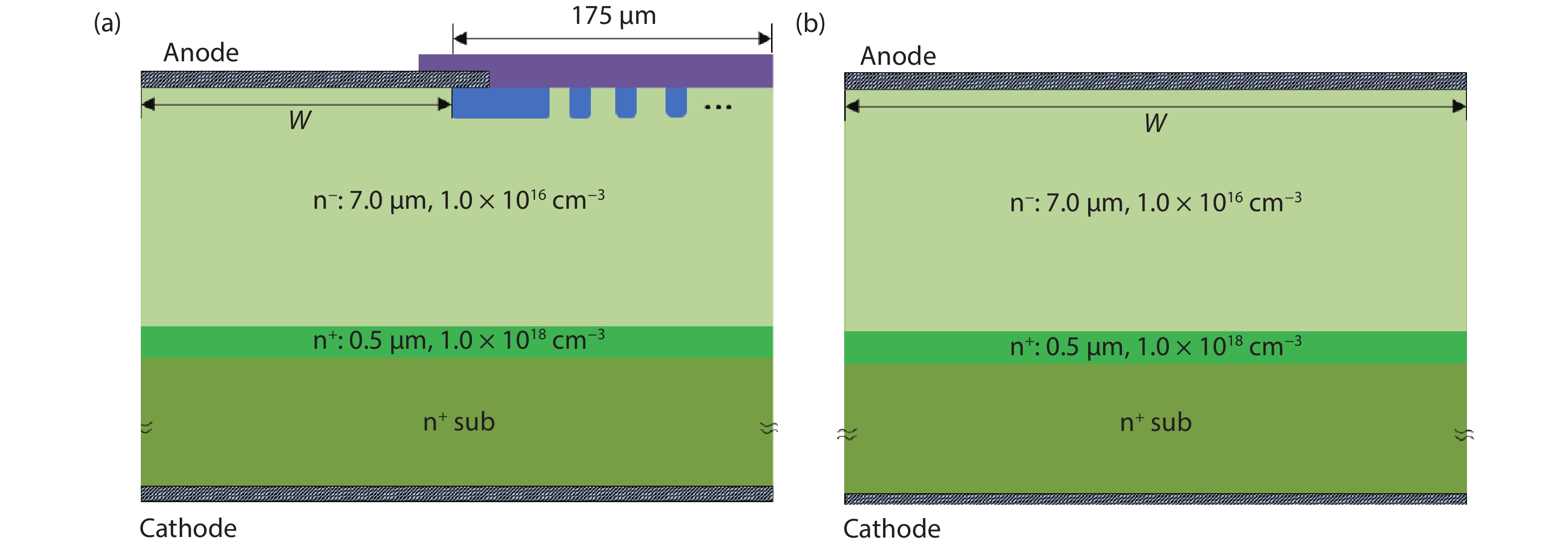
Figure 1.(Color online) Schematics of the device structures used in the simulation. (a) Considering the lateral spreading current. (b) Ignoring the lateral spreading current.
Because the terminal region is included, the forward current of the structure model shown in Fig. 1(a) contains the lateral spreading current. However, the forward current of the structure model shown in Fig. 1(b) does not contain the lateral spreading current. Therefore, proportions of lateral spreading current in the total forward current (Psp) of the devices are extracted through simulation. The values of W and the corresponding chip sizes in the simulation range from 0.325 to 3.325 mm and from 1.0 to 49 mm2, respectively. The simulated relationship between Psp and S is shown in Fig. 2. With the increase in the chip size from 1.0 to 49 mm2, Psp is decreased from 53% to 8%. The simulation results indicate that the value Psp decreases when the SBD chip becomes larger.
![]()
Figure 2.Simulated relationship between chip size and proportion of spread current in the total forward current.
3. Experiment
To further investigate the lateral spreading current, 4H-SiC SBD chips with the same terminal structure are fabricated on a 4-inch 4o off-axis N-type 4H-SiC epitaxial wafer bought from TYSiC Inc. The thickness of the epitaxial layer and the substrate are 7.0 and 350 μm, respectively. There is a 0.5 μm highly doped epitaxial buffer layer between the drift region and the substrate. The doping concentrations of the drift and the buffer layers are 1.0 × 10¹⁶ and 1 × 1018 cm−3, respectively. The FLRs are formed by Al implantation and followed by 1700 °C high-temperature annealing processes, where SiO2 is used as a masking film during the implantation process. A carbon film made by carbonized photoresist is used to protect the 4H-SiC during the high-temperature annealing process. After the annealing process, the carbon film is removed through sacrificial oxidation. Ni, used as the ohmic contact metal, is deposited on the bottom by evaporation equipment. After deposition, a rapid thermal process (RTP) at 1000 °C is carried out to form the ohmic contact. Then, Ni is deposited on the top through the lift-off process and the Schottky contact is formed after RTP. Ag and Al are used as the cathode and anode pads, respectively. Finally, the devices are passivated by SiO2 and polyimide (PI). The chip sizes (S) are 2.0 × 2.0 mm2 and 1.0 × 1.0 mm2. The sizes of the active areas (SA) in the two chips are 1.65 × 1.65 mm2 and 0.65 × 0.65 mm2. Fig. 3 shows the top view of the fabricated SiC SBD chip. It can be seen from the figure that after scribing, the width of the terminal region and scribing trench region is 175 μm.
![]()
Figure 3.(Color online) Top view of the fabricated SiC SBD chip.
After the fabrication processes, the Keysight B1505A power device test system is used to test the SBD chips. The forward and the reverse current–voltage curves of the two chips are shown in Fig. 4. The turn-on voltage of the fabricated SiC SBD chip is about 0.9 V. When the anode voltage is 1.55 V, the forward current of the two SBD chips are 10.7 and 2.5 A. The values of the on-state resistance of the two chips are calculated to be about 145 and 620 mΩ. When the cathode voltage is 650 V, the reverse leakage currents of the two chips are 1.07 and 0.17 μA. Since the chip sizes are different, the forward current (IF) and the leakage current (IR) between the two SBD chips are different. The SBD with a larger chip size shows higher current values.
![]()
Figure 4.(Color online) Current–voltage curves of the fabricated SBD chips. (a) Forward current–voltage curves. (b) Reverse current–voltage curves.
4. Analysis and discussion
Fig. 5 shows the current density-voltage curves of the fabricated SBD chips. Although the vertical parameters and the fabrication processes are the same, both forward current densities (JF = IF/S) and reverse current densities (JR = IR/S) between the two chips are different. Figs. 5(a) and 5(c) show that the SBD with a larger chip size shows higher forward and reverse current densities. In Figs. 5(b) and 5(d) , the current densities are expressed using SA as
![]()
Figure 5.(Color online) Current density–voltage curves of the fabricated SBD chips. (a) Forward current density–voltage curves. (b)
and
respectively. The calculated forward current density (JFA) in the SBD with a smaller chip size is higher. Meanwhile, the calculated reverse current densities (JRA) in the two SBD chips are almost the same. The different results may be caused by the lateral spreading current in the terminal region. When calculating the current densities using SA, the conduction area in the terminal region is ignored. However, the contribution of the conduction area in the terminal region on the forward current is included. Therefore, the SBD with a smaller chip size shows a higher forward calculated value. Meanwhile, the reverse calculated value is almost the same as shown in Fig. 5(d). It is because the reverse leakage current is very small and there is almost no lateral spreading during the reverse biased condition. Although, the current density calculating method that uses SA is incorrect in analyzing the SiC SBD chips, the method is useful for analyzing the lateral spreading current.
Fig. 6 shows the schematic diagrams of the lateral current spreading in the 4H-SiC SBD chips. In the 4H-SiC SBD chip, the entire bottom is covered by a cathode electrode, at the same time, the anode electrode area at the top is depending on the active area. As a result, the top anode electrode and the bottom cathode electrode in the 4H-SiC SBD chip are asymmetrical. Therefore, there are potential and electron density differences at the edge of the active area in the 4H-SiC SBD at on-state. The potential and the electron density differences cause the lateral transport of electrons. The lateral transport of electrons leads to spreading current at the terminal region of the active area. Then, according to the current flowing path, the total forward current (IF) can be divided into two portions. One is the current that flows through the active area and the other is the current that flows through the spreading area under the terminal region. Therefore, the total forward current (IF) of the SBD chip can be defined as the sum of two portions:
![]()
Figure 6.(Color online) Schematic diagrams of the lateral current spreading in the 4H-SiC SBD chip. (a) Cross-section view. (b) Vertical view.
where IA and Isp are the currents that flow through the active and the terminal regions, respectively.
Since IF consists of IA and Isp, a new equation can be achieved by substituting Eq. (3) into Eq. (1)
If the process deviation during the fabrication is ignored, the current density that flows through the active region is a fixed value. Then, IA/SA in the two SBD chips should be the same. Subtracting JFA1 of the larger SBD chip from JFA2 of the smaller SBD chip, the result can be written as:
where Isp1 and SA1 are the spreading current and the active area in the SBD chip with larger size, respectively. While Isp2 and SA2 are the spreading current and the active area in the SBD chip with smaller size, respectively. The values of SA1 and SA2 in this work are 0.027225 and 0.004225 cm2, respectively.
In order to further analyze the lateral spreading current in the 4H-SiC SBD chip, a new parameter needs to be defined to describe the contribution of the spreading current along the edge around the active area. Since the total spreading current Isp is a sum of the extended currents in each region along the active boundary, the linear density of the lateral spreading current along the active boundary (Jsp) is defined in the SBD chips. Thus, the total spreading current in the SBD chip can be expressed as the product of Jsp and the length of the active boundary. The length of the active boundary is scilicet the perimeter of the active area. Considering the vertical parameters, the terminal structure and the fabrication process are all the same in the two SBD chips, and Jsp in the two SBD chips can be approximately equal[
where CA1 and CA2 are the perimeters of the active area in the two 4H-SiC SBD chips. The values of CA1 and CA2 in this paper are 0.66 and 0.26 cm, respectively. Then, from Eqs. (1) and (6), Jsp can be written as:
Then, the value of Isp and the proportion of Isp in the total forward current (Psp) of the SBD chip can be calculated as:
and
respectively. According to Eqs. (8) and (9), Jsp and Psp of the fabricated SiC SBD chips at different anode voltages are calculated and shown in Fig. 7. The calculated Jsp exhibits a linear relation with the anode voltage, indicating that there is a fixed spreading resistance at the on-state in the current spreading region. Therefore, the linear specific spreading resistance in the current spreading region at the on-state can be calculated through the Jsp curve in Fig. 7. The calculated value of linear specific spreading resistance is about 8.6 Ω/cm. Even though the spreading resistance is fixed for a specific chip, the Psp is still increased with the increase in the anode voltage during the initial on-state. Once the anode voltage becomes higher, the increasing rate of Psp slows down and Psp tends to a stable value. As shown in Fig. 7, Psp in the two fabricated chips tends to be stable at the forward voltage drops of 1.5 and 1.55 V with stable values of about 54% and 32%, respectively.
![]()
Figure 7.(Color online) Calculated
For SiC SBDs with different chip sizes, the proportions of the active area in the entire chips are different. The expected active area, the terminal region and the scribing trench also occupy a certain proportion in the entire chip. The proportions of the terminal region and the scribing trench in the entire chip may be concerned with the lateral spreading current. Therefore, Ksp is defined as the proportion of the terminal region and the scribing trench in the entire chip in this work. ThenKsp can be calculated as:
where SA and S are the active and the chip areas, respectively. According to Eq. (10), Ksp for SiC SBDs with different chip sizes can be theoretically calculated assuming that these SBD chips have the same vertical parameters, the same terminal structures and the same fabrication processes. The relation curve of calculated Ksp and S for SiC SBDs with different chip sizes is shown in Fig. 8. It can be seen from the figure that when the size of the SiC SBD chip is small, the active area is small and the proportion of terminal and scribing trench is large. With the increase in the chip size, Ksp decreases. Fig. 8 shows that Ksp is lower than 20% when the chip area is larger than 0.1 cm2. The values of Psp of the simulated SBD chips and the fabricated SBD chips are also calculated and marked in Fig. 8. It is clear that not all the terminal regions and the scribing trenches are effectively contributed to the lateral spreading current. Therefore, there is a relation coefficient between Psp and Ksp. The marked Psp comparatively coincides with the Ksp curve. In the SiC SBDs with chip sizes of 2.0 × 2.0 mm2 and 1.0 × 1.0 mm2, the calculated values of Ksp are 31.94% and 57.75%, respectively. Comparing the calculated Ksp and Psp in the two chips, the values are closed in each chip. For the SBD chip with a chip size of 2.0 × 2.0 mm2, the calculated Psp is slightly higher than Ksp. Meanwhile, for the SBD chip with a chip size of 1.0 × 1.0 mm2, the calculated Psp is slightly lower than Ksp. The difference between the calculated Psp and Ksp may be caused by process deviation during the fabrication and relation coefficient between Psp and Ksp. According to Ksp–S curve, it can be predicted that when the chip area of the fabricated SiC SBD becomes larger than 0.1 cm2, the value of Psp would be lower than 20%. When the chip area of the fabricated SiC SBD becomes larger than 0.5 cm2, the value of Psp would be lower than 10%.
![]()
Figure 8.
5. Conclusion
In this paper, the lateral current spreading in the 4H-SiC SBD chip is investigated through simulation and experiment. The obtained results indicate that there is a fixed spreading resistance at the on-state in the current spreading region. The linear specific spreading resistance at the on-state is calculated to be about 8.6 Ω/cm in the fabricated chips. Moreover, the proportion of the lateral spreading current in the total forward current (Psp) is related to both the anode voltage and chip area. During the initial on-state,Psp increases with the increase in the anode voltage. Then Psp tends to a stable value. The stable values of Psp of the two fabricated chips are about 32% and 54%. The calculated proportions of the terminal region and the scribing trench in the entire chip (Ksp) of the two fabricated chips are 31.94% and 57.75%, respectively, which are closed with Psp in a specific chip. The calculated Ksp can be used to predict Psp in the SiC SBD chips with different sizes. When the chip area of the fabricated SiC SBD becomes larger than 0.5 cm2, the value of Psp would be lower than 10%. The results obtained in this work can be introduced to the lateral spreading current investigations in other SiC power devices.
Acknowledgements
This work was supported in part by National Natural Science Foundation of China (62004161), in part by Natural Science Basic Research Plan in Shaanxi Province of China (2020JQ-636), in part by Scientific Research Project of Education Department of Shaanxi Province (20JK0796), in part by Youth talent lift project of Xi’an Science and Technology Association (095920201318) and in part by Bidding Project of Shanxi Province (20201101017).
References
[1] T Kimoto, Y Yonezawa. Current status and perspectives of ultrahigh-voltage SiC power devices. Mater Sci Semicond Process, 78, 43(2018).
[2] X B Yuan, I Laird, S Walder. Opportunities, challenges, and potential solutions in the application of fast-switching SiC power devices and converters. IEEE Trans Power Electron, 36, 3925(2021).
[3] H Z Liu, J Wang, S W Liang et al. Physical modeling and design optimization of 4H-SiC insulated gate bipolar transistors for d
[4] J L Li, C X Meng, L Yu et al. Effect of various defects on 4H-SiC Schottky diode performance and its relation to epitaxial growth conditions. Micromachines, 11, 609(2020).
[5] P A Ivanov, A S Potapov, N M Lebedeva et al. Avalanche breakdown in 4H-SiC Schottky diodes: Reliability aspects. Tech Phys, 65, 2041(2020).
[6] X Wang, H B Pu, Q Liu et al. Demonstration of 4H-SiC thyristor triggered by 100-mW/cm2 UV light. IEEE Electron Device Lett, 41, 824(2020).
[7] R Rupp, M Treu, A Mauder et al. Performance and reliability issues of SiC-Schottky diodes. Mater Sci Forum, 338–342, 1167(2000).
[8] X B Yuan, S Walder, N Oswald. EMI generation characteristics of SiC and Si diodes: Influence of reverse-recovery characteristics. IEEE Trans Power Electron, 30, 1131(2015).
[9] L Liu, J P Wu, N Ren et al. 1200-V 4H-SiC merged p-i-n Schottky diodes with high avalanche capability. IEEE Trans Electron Devices, 67, 3679(2020).
[10] B Zaťko, L Hrubčín, A Šagátová et al. Study of Schottky barrier detectors based on a high quality 4H-SiC epitaxial layer with different thickness. Appl Surf Sci, 536, 147801(2021).
[11] P V Raja, N V L Narasimha Murty. Thermally annealed gamma irradiated Ni/4H-SiC Schottky barrier diode characteristics. J Semicond, 40, 022804(2019).
[12] H Yuan, Y C Liu, Y J He et al. Characteristic and robustness of trench floating limiting rings for 4H-SiC junction barrier Schottky rectifiers. IEEE Electron Device Lett, 41, 1056(2020).
[13] R Elpelt, M Draghici, R Gerlach et al. SiC MPS devices: One step closer to the ideal diode. Mater Sci Forum, 924, 609(2018).
[14] S Palanisamy, J Kowalsky, J Lutz et al. Repetitive surge current test of SiC MPS diode with load in bipolar regime. 2018 IEEE 30th International Symposium on Power Semiconductor Devices and ICs (ISPSD), 367(2018).
[15] Q W Song, H Yuan, Q J Sun et al. Reverse-bias stress-induced electrical parameters instability in 4H-SiC JBS diodes terminated nonequidistance FLRs. IEEE Trans Electron Devices, 66, 3935(2019).
[16] Q Zhang, T S Sudarshan. Lateral current spreading in SiC Schottky diodes using metal overlap edge termination. Solid State Electron, 45, 1847(2001).
[17]
[18] I G Ivanov, A Henry, E Janzén. Ionization energies of phosphorus and nitrogen donors and aluminum acceptors in 4H silicon carbide from the donor-acceptor pair emission. Phys Rev B, 71, 241201(2005).
[19] D Stefanakis, K Zekentes. TCAD models of the temperature and doping dependence of the bandgap and low field carrier mobility in 4H-SiC. Microelectron Eng, 116, 65(2014).
[20] Y Zhao, H Niwa, T Kimoto. Impact ionization coefficients of 4H-SiC in a wide temperature range. Jpn J Appl Phys, 58, 018001(2019).
[21]
[22] L Zhu, T P Chow. Analytical modeling of high-voltage 4H-SiC junction barrier Schottky (JBS) rectifiers. IEEE Trans Electron Devices, 55, 1857(2008).
[23] N Ren, K Sheng. An analytical model with 2-D effects for 4H-SiC trenched junction barrier Schottky diodes. IEEE Trans Electron Devices, 61, 4158(2014).

Set citation alerts for the article
Please enter your email address
© Copyright 2018-2021 | Chinese Laser Press. All Rights Reserved 沪ICP备15018463号-20