• Photonics Research
  • Vol. 10, Issue 7, 1744 (2022)
Jingyu Wang1、†, Weimin Yang1、†, Guoya Sun1、2、*, Yonglin He1, Peiwen Ren1, and Zhilin Yang1、3、*
Author Affiliations
  • 1Department of Physics, Collaborative Innovation Center for Optoelectronic Semiconductors and Efficient Devices, Jiujiang Research Institute, Xiamen University, Xiamen 361005, China
  • 2e-mail: gysun@xmu.edu.cn
  • 3e-mail: zlyang@xmu.edu.cn
  • show less
    DOI: 10.1364/PRJ.453099 Cite this Article Set citation alerts
    Jingyu Wang, Weimin Yang, Guoya Sun, Yonglin He, Peiwen Ren, Zhilin Yang. Boosting anapole-exciton strong coupling in all-dielectric heterostructures[J]. Photonics Research, 2022, 10(7): 1744 Copy Citation Text show less
    (a) Schematic illustration of the Si nanodisk-bulk WS2 heterostructure array under normally incident illumination with a radius R and a height H of Si nanodisks, and a radius r and a height h of bulk WS2. (b) Schematic illustration of the strong interplay between the anapole state in the Si nanodisk and the bulk WS2 exciton, leading to hybrid states with a large Rabi splitting.
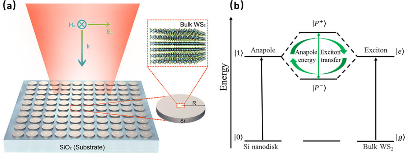
    Fig. 1. (a) Schematic illustration of the Si nanodisk-bulk WS2 heterostructure array under normally incident illumination with a radius R and a height H of Si nanodisks, and a radius r and a height h of bulk WS2. (b) Schematic illustration of the strong interplay between the anapole state in the Si nanodisk and the bulk WS2 exciton, leading to hybrid states with a large Rabi splitting.
    Analyses of the nonradiating anapole mode in the heterostructures. (a) Simulated transmission contour map as a function of radius of the Si nanodisk array (R=100–200 nm), where the height of the Si nanodisk H=70 nm. (b) Simulated transmission contour map as a function of height of the Si nanodisk array (H=20–80 nm), where the radius of the Si nanodisk R=130 nm. (c) Simulated transmission spectrum of the Si nanodisk array (blue solid curve); the Si nanodisk array with air hole, where the radius of air hole is 50 nm, the height is 70 nm, and radius of the Si nanodisk R=130 nm (red solid curve); and the Si nanodisk-bulk WS2 heterostructure array, where f0=0 (black solid curve). The electric-field enhancement distribution in the x−y plane (upper panels) and the magnetic-field enhancement distribution in the y−z plane (lower panels) of the anapole mode for the (d) Si nanodisk array, (e) the Si nanodisk array with air holes, and (f) the Si nanodisk-bulk WS2 heterostructure array, where f0=0. The black arrows represent the magnetic dipole M in lower panels of (d)–(f).
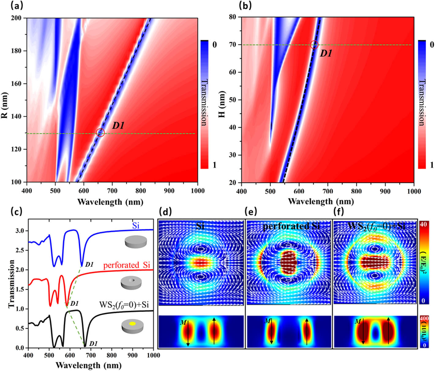
    Fig. 2. Analyses of the nonradiating anapole mode in the heterostructures. (a) Simulated transmission contour map as a function of radius of the Si nanodisk array (R=100200  nm), where the height of the Si nanodisk H=70  nm. (b) Simulated transmission contour map as a function of height of the Si nanodisk array (H=2080  nm), where the radius of the Si nanodisk R=130  nm. (c) Simulated transmission spectrum of the Si nanodisk array (blue solid curve); the Si nanodisk array with air hole, where the radius of air hole is 50 nm, the height is 70 nm, and radius of the Si nanodisk R=130  nm (red solid curve); and the Si nanodisk-bulk WS2 heterostructure array, where f0=0 (black solid curve). The electric-field enhancement distribution in the xy plane (upper panels) and the magnetic-field enhancement distribution in the yz plane (lower panels) of the anapole mode for the (d) Si nanodisk array, (e) the Si nanodisk array with air holes, and (f) the Si nanodisk-bulk WS2 heterostructure array, where f0=0. The black arrows represent the magnetic dipole M in lower panels of (d)–(f).
    (a) Normalized Cartesian multipole decomposition results for the Si nanodisk-bulk WS2 heterostructure array, where the radius of center WS2 is 50 nm and the height is 70 nm, which is treated as background index-only material. The inset presents the normalized scattered power in the wavelength range 630−670 nm. (b) Corresponding normalized phase of P and T for the structure of (a).
    Fig. 3. (a) Normalized Cartesian multipole decomposition results for the Si nanodisk-bulk WS2 heterostructure array, where the radius of center WS2 is 50 nm and the height is 70 nm, which is treated as background index-only material. The inset presents the normalized scattered power in the wavelength range 630−670 nm. (b) Corresponding normalized phase of P and T for the structure of (a).
    Analyses of the resonance coupling in the heterostructures, where the excitonic effect of bulk WS2 is considered (f0=0.4). (a) Simulated transmission contour map as a function of radius of the Si nanodisk (R=80–200 nm), where the height of the Si nanodisk H=70 nm, the radius of bulk WS2 is r=50 nm, and the height is h=70 nm. (b) The energy of the upper branch (UB) (red sphere) and lower branch (LB) (blue sphere) as a function of detuning. The solid lines are fit to the coupled oscillator model, giving a splitting of 151 meV. (c) Simulated transmission spectrum of the Si nanodisk-bulk WS2 heterostructure array when R=130 nm and r=50 nm, where the f0 is set as 0 (black dash line) and 0.4 (red solid line). The electric-field enhancement distribution in the x−y plane (upper panels) and the magnetic-field enhancement distribution in the y−z plane (lower panels) at the (d) UB and (e) LB for the structure of (c).
    Fig. 4. Analyses of the resonance coupling in the heterostructures, where the excitonic effect of bulk WS2 is considered (f0=0.4). (a) Simulated transmission contour map as a function of radius of the Si nanodisk (R=80200  nm), where the height of the Si nanodisk H=70  nm, the radius of bulk WS2 is r=50  nm, and the height is h=70  nm. (b) The energy of the upper branch (UB) (red sphere) and lower branch (LB) (blue sphere) as a function of detuning. The solid lines are fit to the coupled oscillator model, giving a splitting of 151 meV. (c) Simulated transmission spectrum of the Si nanodisk-bulk WS2 heterostructure array when R=130  nm and r=50  nm, where the f0 is set as 0 (black dash line) and 0.4 (red solid line). The electric-field enhancement distribution in the xy plane (upper panels) and the magnetic-field enhancement distribution in the yz plane (lower panels) at the (d) UB and (e) LB for the structure of (c).
    Wavelength dependence of the (a), (b) real and (c), (d) imaginary parts of the in-plane complex index of refraction for a Lorentz model dielectric of bulk WS2 with (a), (c) f0=0 and (b), (d) f0=0.4.
    Fig. 5. Wavelength dependence of the (a), (b) real and (c), (d) imaginary parts of the in-plane complex index of refraction for a Lorentz model dielectric of bulk WS2 with (a), (c) f0=0 and (b), (d) f0=0.4.
    (a) Simulated scattering spectrum of isolated, 3×3 finite number of unit cell and 5×5 finite number of unit cell for Si nanodisk-bulk WS2 heterostructure with R=130 nm, H=70 nm, r=50 nm, and f0=0. (b) The electric-field enhancement distribution in the x−y plane at the resonance wavelength of the isolated heterostructure. (c) The electric-field enhancement distribution in the x−y plane at the resonance wavelength of 3×3 finite number of unit cells for the heterostructure. (d) The electric-field enhancement distribution in the x−y plane at the resonance wavelength of 5×5 finite number of unit cells for the heterostructure. (e) The electric-field enhancement distribution in the x−y plane at the resonance wavelength of the heterostructure array with Λ=500 nm.
    Fig. 6. (a) Simulated scattering spectrum of isolated, 3×3 finite number of unit cell and 5×5 finite number of unit cell for Si nanodisk-bulk WS2 heterostructure with R=130  nm, H=70  nm, r=50  nm, and f0=0. (b) The electric-field enhancement distribution in the xy plane at the resonance wavelength of the isolated heterostructure. (c) The electric-field enhancement distribution in the xy plane at the resonance wavelength of 3×3 finite number of unit cells for the heterostructure. (d) The electric-field enhancement distribution in the xy plane at the resonance wavelength of 5×5 finite number of unit cells for the heterostructure. (e) The electric-field enhancement distribution in the xy plane at the resonance wavelength of the heterostructure array with Λ=500  nm.
    (a) Simulated transmission spectrum for Si nanodisk-bulk WS2 (f0=0) heterostructure arrays with different periodicities. The near-field distribution of WS2 (f0=0)-Si nanodisk heterostructure arrays with periodicity of (b) 300 nm, (c) 400 nm, (d) 500 nm, (e) 600 nm, and (f) 700 nm at the position of the exciton absorption peak of around 656 nm.
    Fig. 7. (a) Simulated transmission spectrum for Si nanodisk-bulk WS2 (f0=0) heterostructure arrays with different periodicities. The near-field distribution of WS2 (f0=0)-Si nanodisk heterostructure arrays with periodicity of (b) 300 nm, (c) 400 nm, (d) 500 nm, (e) 600 nm, and (f) 700 nm at the position of the exciton absorption peak of around 656 nm.
    (a) Normalized corresponding transmission spectra and contributions from different multipoles for the Si nanodisk-bulk WS2 (f0=0) heterostructure array. (b) Total scattering power and contributions from different multipoles for the Si nanodisk-bulk WS2 (f0=0) heterostructure array.
    Fig. 8. (a) Normalized corresponding transmission spectra and contributions from different multipoles for the Si nanodisk-bulk WS2 (f0=0) heterostructure array. (b) Total scattering power and contributions from different multipoles for the Si nanodisk-bulk WS2 (f0=0) heterostructure array.
    Simulated transmission contour map as a function of radius of the Si nanodisk (R=100–200 nm) for the Si nanodisk-bulk WS2 heterostructure array, where bulk WS2 is treated as background index-only material.
    Fig. 9. Simulated transmission contour map as a function of radius of the Si nanodisk (R=100200  nm) for the Si nanodisk-bulk WS2 heterostructure array, where bulk WS2 is treated as background index-only material.
    (a) Simulated transmission contour map as a function of radius of the WS2 (r=40–100 nm) for the Si nanodisk-bulk WS2 heterostructure array, where bulk WS2 is treated as background index-only material, the radius of Si nanodisk is R=130 nm, and the height H=70 nm. (b) Simulated transmission contour map as a function of radius of the WS2 (r=40–100 nm) for the Si nanodisk-bulk WS2 heterostructure array, where the exciton of bulk WS2 is considered, the radius of Si nanodisk is R=130 nm, and the height H=70 nm. The electric-field enhancement distribution in the x−y plane for an individual nanodisk of the heterostructure array with WS2 radius (c) 20 nm, (d) 50 nm, and (e) 100 nm.
    Fig. 10. (a) Simulated transmission contour map as a function of radius of the WS2 (r=40100  nm) for the Si nanodisk-bulk WS2 heterostructure array, where bulk WS2 is treated as background index-only material, the radius of Si nanodisk is R=130  nm, and the height H=70  nm. (b) Simulated transmission contour map as a function of radius of the WS2 (r=40100  nm) for the Si nanodisk-bulk WS2 heterostructure array, where the exciton of bulk WS2 is considered, the radius of Si nanodisk is R=130  nm, and the height H=70  nm. The electric-field enhancement distribution in the xy plane for an individual nanodisk of the heterostructure array with WS2 radius (c) 20 nm, (d) 50 nm, and (e) 100 nm.
    (a) Simulated transmission contour map as a function of f for Si nanodisk-bulk WS2 heterostructure array. (b) In-plane (Re[n]) dielectric functions of bulk WS2 with different f.
    Fig. 11. (a) Simulated transmission contour map as a function of f for Si nanodisk-bulk WS2 heterostructure array. (b) In-plane (Re[n]) dielectric functions of bulk WS2 with different f.
    (a) Simulated transmission contour map as a function of radius of the Si nanodisk (R=50–200 nm) for the Si nanodisk-bulk WS2 heterostructure array, where bulk WS2 is positioned on top of the Si nanodisk surface, the radius of WS2 is r=50 nm, and f0 is set as 0.4. (b) Simulated transmission contour map as a function of radius of the Si nanodisk (R=50–200 nm) for Si nanodisk-bulk WS2 heterostructure array, where bulk WS2 is positioned on the side surface of the Si nanodisk, the width of WS2 is 50 nm, and f0 is set as 0.4.
    Fig. 12. (a) Simulated transmission contour map as a function of radius of the Si nanodisk (R=50200  nm) for the Si nanodisk-bulk WS2 heterostructure array, where bulk WS2 is positioned on top of the Si nanodisk surface, the radius of WS2 is r=50  nm, and f0 is set as 0.4. (b) Simulated transmission contour map as a function of radius of the Si nanodisk (R=50200  nm) for Si nanodisk-bulk WS2 heterostructure array, where bulk WS2 is positioned on the side surface of the Si nanodisk, the width of WS2 is 50 nm, and f0 is set as 0.4.
    (a) Simulated transmission spectrum of the Si nanodisk array, where the radius of the Si nanodisk is R=150 nm, the height is 70 nm, and the period is Λ=500 nm. The inset shows the electric-field enhancement distribution of the anapole mode. (b) Simulated transmission contour map of the Si nanodisk-J-Aggregate heterostructure array as a function of radius of the Si nanodisk (R=100–200 nm), where the height of the Si nanodisk H=70 nm and the radius of the J-Aggregates is 40 nm.
    Fig. 13. (a) Simulated transmission spectrum of the Si nanodisk array, where the radius of the Si nanodisk is R=150  nm, the height is 70 nm, and the period is Λ=500  nm. The inset shows the electric-field enhancement distribution of the anapole mode. (b) Simulated transmission contour map of the Si nanodisk-J-Aggregate heterostructure array as a function of radius of the Si nanodisk (R=100200  nm), where the height of the Si nanodisk H=70  nm and the radius of the J-Aggregates is 40 nm.
    Jingyu Wang, Weimin Yang, Guoya Sun, Yonglin He, Peiwen Ren, Zhilin Yang. Boosting anapole-exciton strong coupling in all-dielectric heterostructures[J]. Photonics Research, 2022, 10(7): 1744
    Download Citation