• Photonics Research
  • Vol. 11, Issue 5, 695 (2023)
Zhengchang Liu1、†, Zhibo Dang1、†, Zhixin Liu, Yu Li, Xiao He, Yuchen Dai, Yuxiang Chen, Pu Peng, and Zheyu Fang*
Author Affiliations
  • School of Physics, State Key Lab for Mesoscopic Physics, Academy for Advanced Interdisciplinary Studies, Collaborative Innovation Center of Quantum Matter, Yangtze Delta Institute of Optoelectronics, and Nano-optoelectronics Frontier Center of Ministry of Education, Peking University, Beijing 100871, China
  • show less
    DOI: 10.1364/PRJ.480845 Cite this Article Set citation alerts
    Zhengchang Liu, Zhibo Dang, Zhixin Liu, Yu Li, Xiao He, Yuchen Dai, Yuxiang Chen, Pu Peng, Zheyu Fang. Self-design of arbitrary polarization-control waveplates via deep neural networks[J]. Photonics Research, 2023, 11(5): 695 Copy Citation Text show less
    Schematic of the self-designed platform Bayesian optimization-net (BO-Net). (a) Left: the schematic of the self-designed waveplate, consisting of a metal-insulator-metal (MIM) unit cell. Right: the binary matrix parameterization. The shape of the top nanostructures is described by a 40×40 matrix, where 1 (0) represents a square column of Au (air) with a size of 10 nm×10 nm×40 nm. (b) The architecture of the deep neural networks (DNNs) and the BO. The upper part displays the workflow of the DNNs, including two kinds of network layers. The convolution layers extract the structure of the geometric features related to the optical properties. The dense layers are used to map these features to the response of the reflection spectra. The lower part displays the workflow of the BO. The Bayesian statistical model estimates the predicted function with a 95% confidence interval to approximate the objective function through Gaussian processes. The utility function can be extracted from the upper bound of the 95% confidence interval. Based on the local maxima of the utility function (denoted by stars) in the whole design space, the probabilistic optimal structures for the next generation can be recommended. (c) The schematic of the final generated nanostructures with the target optical response, which can act as a unit cell.
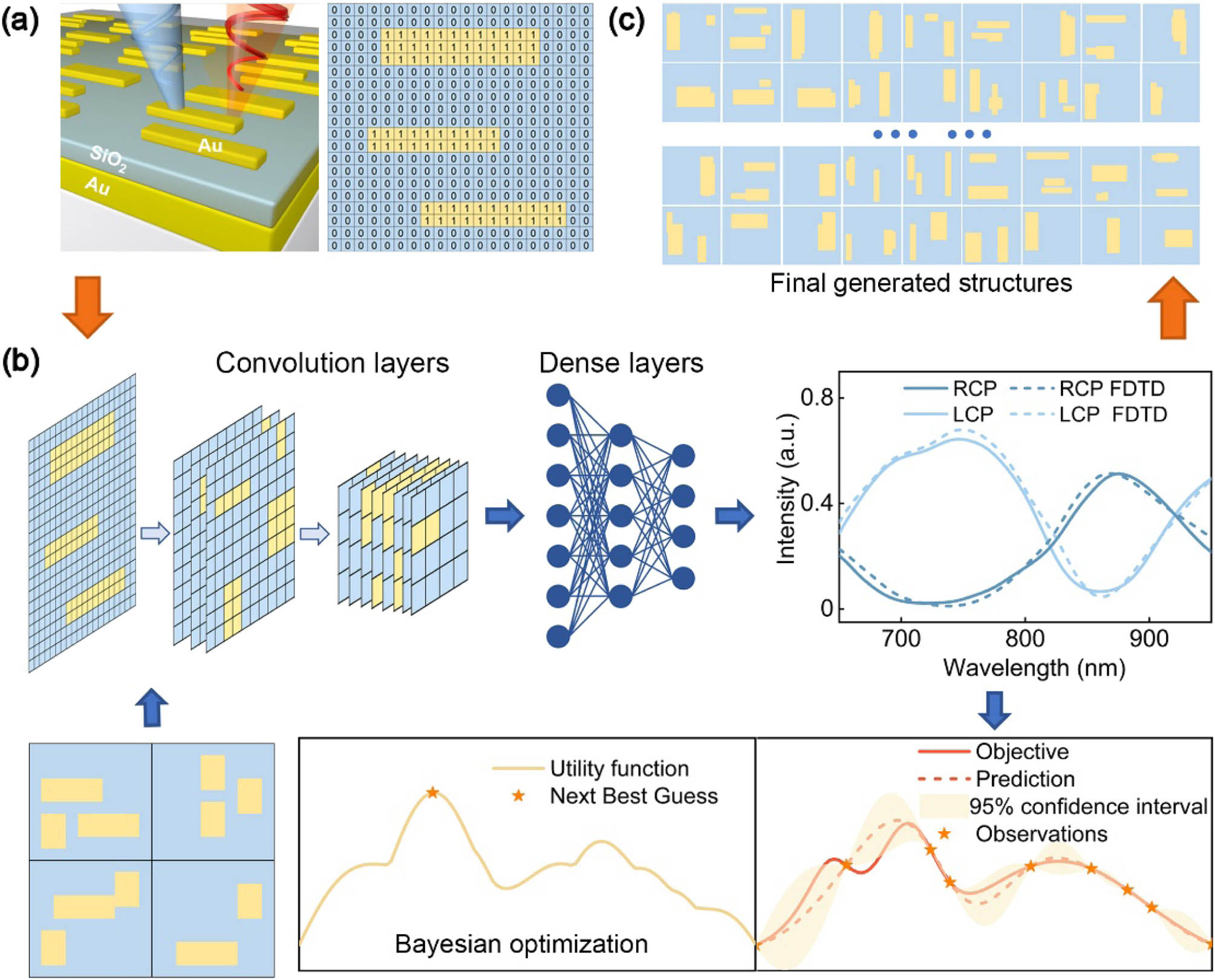
    Fig. 1. Schematic of the self-designed platform Bayesian optimization-net (BO-Net). (a) Left: the schematic of the self-designed waveplate, consisting of a metal-insulator-metal (MIM) unit cell. Right: the binary matrix parameterization. The shape of the top nanostructures is described by a 40×40 matrix, where 1 (0) represents a square column of Au (air) with a size of 10  nm×10  nm×40  nm. (b) The architecture of the deep neural networks (DNNs) and the BO. The upper part displays the workflow of the DNNs, including two kinds of network layers. The convolution layers extract the structure of the geometric features related to the optical properties. The dense layers are used to map these features to the response of the reflection spectra. The lower part displays the workflow of the BO. The Bayesian statistical model estimates the predicted function with a 95% confidence interval to approximate the objective function through Gaussian processes. The utility function can be extracted from the upper bound of the 95% confidence interval. Based on the local maxima of the utility function (denoted by stars) in the whole design space, the probabilistic optimal structures for the next generation can be recommended. (c) The schematic of the final generated nanostructures with the target optical response, which can act as a unit cell.
    Variation of the polarization conversion efficiency (PCE) during the optimization process. (a) The reflection spectrum of a given nanostructure for the left-handed circularly polarized (LCP) planewave, calculated by DNNs (solid lines) and FDTD (dashed lines). The inset displays the geometric morphology of the corresponding nanostructure. (b) The maximum of the PCE as a function of generations. The PCE (averaged by wavelength) of each nanostructure generated during the optimization process is recorded as a function of generations (the number of iterations). The inset shows the five-number (the minimum, first quartile, median, third quartile, and the maximum) summary of the PCE data in the first 5 generations. The vertical line through the box indicates the median, the whiskers from each quartile indicate the minimum or the maximum, and the box indicates the value range of 50% PCE distribution. (c) The PCR spectrum of the representative nanostructures selected from the first 9 generations, labeled from G1 to G9. The side panel displays the corresponding geometric morphology of G1–G9, in the order from bottom to top.
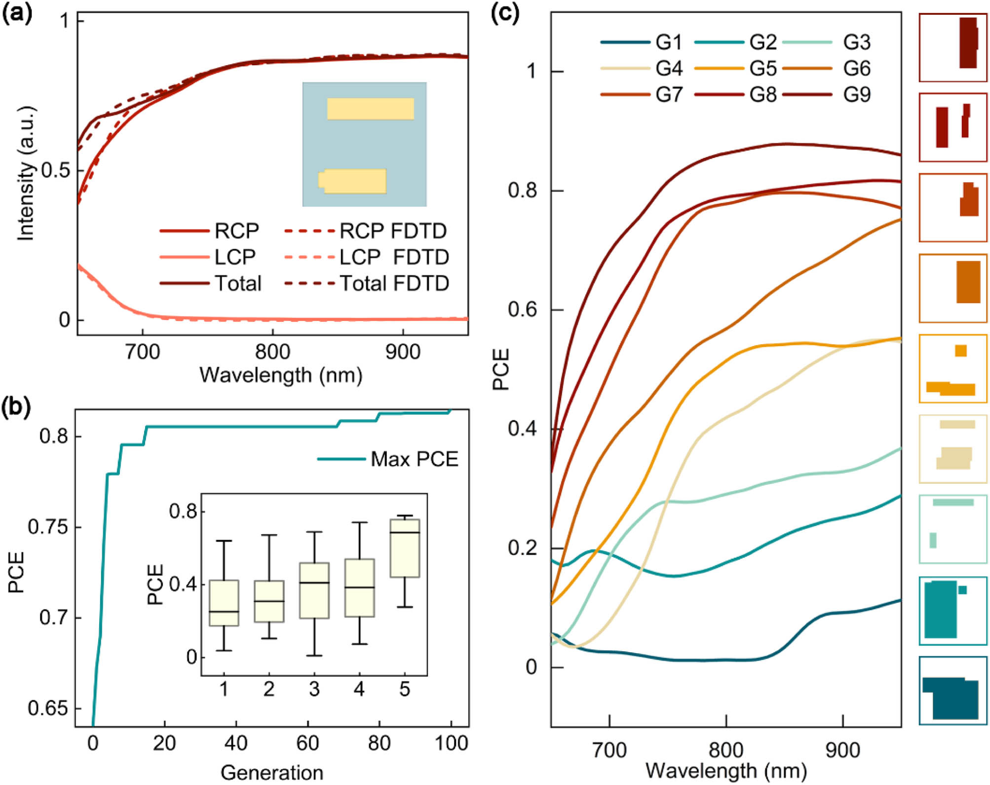
    Fig. 2. Variation of the polarization conversion efficiency (PCE) during the optimization process. (a) The reflection spectrum of a given nanostructure for the left-handed circularly polarized (LCP) planewave, calculated by DNNs (solid lines) and FDTD (dashed lines). The inset displays the geometric morphology of the corresponding nanostructure. (b) The maximum of the PCE as a function of generations. The PCE (averaged by wavelength) of each nanostructure generated during the optimization process is recorded as a function of generations (the number of iterations). The inset shows the five-number (the minimum, first quartile, median, third quartile, and the maximum) summary of the PCE data in the first 5 generations. The vertical line through the box indicates the median, the whiskers from each quartile indicate the minimum or the maximum, and the box indicates the value range of 50% PCE distribution. (c) The PCR spectrum of the representative nanostructures selected from the first 9 generations, labeled from G1 to G9. The side panel displays the corresponding geometric morphology of G1–G9, in the order from bottom to top.
    Reflection measurement results and the characterization of the optimized database. (a) The measured PCE spectra of the representative nanostructures from different generations in the half-waveplates (HWPs) design process, labeled as stru1, stru2, stru3, stru4, and stru5 in order of increase in the generations. Side panel: SEM images of the corresponding nanostructures. (b), (c) The measured polarization conversion ratio (PCR) spectra of eight randomly selected unit cells of the HWPs (b) and QWPs (c) from the optimized database. Side panel: SEM images of the corresponding structures. (d) The simulated phase shift of the reflected light, which is introduced by the nanostructures in the optimized database. Each pixel corresponds to a nanostructure in the optimized database, the x coordinate implies the working wavelength of the element, the y coordinate implies the introduced phase shift, and the color indicates the corresponding PCE at the working wavelength. (e) The PCE (averaged by wavelength) versus the group delay for different nanostructures in the optimized database after filtering those with a PCE lower than 5%. Each dot represents a nanostructure with a certain averaged PCE (x coordinate), group delay (y coordinate), and R2 (color bar). Group delay (defined as the slope of fitted line) and R2 can be obtained by employing linear fitting to the phase shift spectra of a certain nanostructure from 650 to 950 nm. The group delay of the nanostructures with over 40% PCE ranges from 0 to 10 fs, demonstrating the potential for constructing achromatic metalenses with both high efficiencies and large numerical apertures. Scale bars, 100 nm.
    Fig. 3. Reflection measurement results and the characterization of the optimized database. (a) The measured PCE spectra of the representative nanostructures from different generations in the half-waveplates (HWPs) design process, labeled as stru1, stru2, stru3, stru4, and stru5 in order of increase in the generations. Side panel: SEM images of the corresponding nanostructures. (b), (c) The measured polarization conversion ratio (PCR) spectra of eight randomly selected unit cells of the HWPs (b) and QWPs (c) from the optimized database. Side panel: SEM images of the corresponding structures. (d) The simulated phase shift of the reflected light, which is introduced by the nanostructures in the optimized database. Each pixel corresponds to a nanostructure in the optimized database, the x coordinate implies the working wavelength of the element, the y coordinate implies the introduced phase shift, and the color indicates the corresponding PCE at the working wavelength. (e) The PCE (averaged by wavelength) versus the group delay for different nanostructures in the optimized database after filtering those with a PCE lower than 5%. Each dot represents a nanostructure with a certain averaged PCE (x coordinate), group delay (y coordinate), and R2 (color bar). Group delay (defined as the slope of fitted line) and R2 can be obtained by employing linear fitting to the phase shift spectra of a certain nanostructure from 650 to 950 nm. The group delay of the nanostructures with over 40% PCE ranges from 0 to 10 fs, demonstrating the potential for constructing achromatic metalenses with both high efficiencies and large numerical apertures. Scale bars, 100 nm.
    Designed achromatic metalens with a polarization conversion function. (a) The schematic of an achromatic metalens designed at the center wavelength of 800 nm with a bandwidth of 200 nm. (b) The magnified view of the metallic nanostructures of a region of the metalens. (c) The required and realized relative group delay from the center to the edge of the achromatic metalens. (d) The realized phase profile (dot lines) and the ideal phase profile (solid lines) at wavelengths of 700 nm, 800 nm, and 900 nm. (e) The simulated intensity distributions in the linear scale of the different wavelengths. The white dashed lines pass through the center of the focal spots in the case of λ=800 nm. (f) The intensity profiles along the white dashed lines of (e).
    Fig. 4. Designed achromatic metalens with a polarization conversion function. (a) The schematic of an achromatic metalens designed at the center wavelength of 800 nm with a bandwidth of 200 nm. (b) The magnified view of the metallic nanostructures of a region of the metalens. (c) The required and realized relative group delay from the center to the edge of the achromatic metalens. (d) The realized phase profile (dot lines) and the ideal phase profile (solid lines) at wavelengths of 700 nm, 800 nm, and 900 nm. (e) The simulated intensity distributions in the linear scale of the different wavelengths. The white dashed lines pass through the center of the focal spots in the case of λ=800  nm. (f) The intensity profiles along the white dashed lines of (e).
    Bandpass left-handed circularly polarized (LCP) cathodoluminescence (CL) images and reflection matrix. (a), (b) Bandpass LCP CL images (scalebar=50 nm) of 4 fabricated nanostructures (2 HWPs: struB and struD and 2 QWPs: struIII and struIV) with a center wavelength at 510 nm and 794 nm. The color implies the intensity of the CL emissions, and the black arrow denotes the left-handed circular polarization. The profile of the nanostructures is outlined by dashed lines. At 794 nm, the distribution of the hot spots shows a chiral feature, implying a strong near-field interaction between the nanostructures and the incident light field. However, hot spots can barely be observed at 510 nm out of the working band. (c), (d) The amplitude of each matrix element (solid lines) and S3 (shadow region) as a function of wavelengths. Rxy is equal to Ryx due to the reciprocity theorem. For the HWPs, Rxx and Ryy stay around 1 over the working band. For the QWPs, S3 changes to −1 after 650 nm, ensuring a nearly perfect RCP light. (e), (f) The phase of the dominant matrix elements as a function of wavelengths. The absolute phase difference between Rxx and Ryy (Ryx) is also plotted as green dashed lines. The horizontal gray line serves as a guide to the eye. For the HWPs, the phase difference stays around π in the working band, and for the QWPs, the phase difference stays around π/2 in the working band, both showing good agreement with numerical predictions.
    Fig. 5. Bandpass left-handed circularly polarized (LCP) cathodoluminescence (CL) images and reflection matrix. (a), (b) Bandpass LCP CL images (scalebar=50  nm) of 4 fabricated nanostructures (2 HWPs: struB and struD and 2 QWPs: struIII and struIV) with a center wavelength at 510 nm and 794 nm. The color implies the intensity of the CL emissions, and the black arrow denotes the left-handed circular polarization. The profile of the nanostructures is outlined by dashed lines. At 794 nm, the distribution of the hot spots shows a chiral feature, implying a strong near-field interaction between the nanostructures and the incident light field. However, hot spots can barely be observed at 510 nm out of the working band. (c), (d) The amplitude of each matrix element (solid lines) and S3 (shadow region) as a function of wavelengths. Rxy is equal to Ryx due to the reciprocity theorem. For the HWPs, Rxx and Ryy stay around 1 over the working band. For the QWPs, S3 changes to 1 after 650 nm, ensuring a nearly perfect RCP light. (e), (f) The phase of the dominant matrix elements as a function of wavelengths. The absolute phase difference between Rxx and Ryy (Ryx) is also plotted as green dashed lines. The horizontal gray line serves as a guide to the eye. For the HWPs, the phase difference stays around π in the working band, and for the QWPs, the phase difference stays around π/2 in the working band, both showing good agreement with numerical predictions.
    Schematic diagram of the deep neural network.
    Fig. 6. Schematic diagram of the deep neural network.
    Loss evolution during the training process on both the training set and the validation set. (a), (b) The loss evolution of the LCP and the RCP spectrum for the half-wave plates (HWPs) design. (c), (d) The loss evolution of the LCP and the RCP spectrum for the quarter-wave plates (QWPs) design.
    Fig. 7. Loss evolution during the training process on both the training set and the validation set. (a), (b) The loss evolution of the LCP and the RCP spectrum for the half-wave plates (HWPs) design. (c), (d) The loss evolution of the LCP and the RCP spectrum for the quarter-wave plates (QWPs) design.
    Variation of the PCE during the optimization process of the QWPs. The PCE (averaged by wavelength) of each nanostructure generated during the optimization process is recorded as a function of generations (the number of iterations). The inset shows the five-number (the minimum, first quartile, median, third quartile, and the maximum) summary of the PCE data in the first 5 generations. The vertical line through the box indicates the median, the whiskers from each quartile indicate the minimum or the maximum, and the box indicates the value range of 50% PCE distribution.
    Fig. 8. Variation of the PCE during the optimization process of the QWPs. The PCE (averaged by wavelength) of each nanostructure generated during the optimization process is recorded as a function of generations (the number of iterations). The inset shows the five-number (the minimum, first quartile, median, third quartile, and the maximum) summary of the PCE data in the first 5 generations. The vertical line through the box indicates the median, the whiskers from each quartile indicate the minimum or the maximum, and the box indicates the value range of 50% PCE distribution.
    Examples of the optimized nanostructures in our database. (a)–(f) The reflection spectrum of a given nanostructure (inset) under a normally incident LCP planewave, calculated by the DNNs (solid lines) and the FDTD simulations (dashed lines). (a)–(d) These nanostructures are fabricated and measured, and the results are shown in the main text.
    Fig. 9. Examples of the optimized nanostructures in our database. (a)–(f) The reflection spectrum of a given nanostructure (inset) under a normally incident LCP planewave, calculated by the DNNs (solid lines) and the FDTD simulations (dashed lines). (a)–(d) These nanostructures are fabricated and measured, and the results are shown in the main text.
    Examples of the optimized nanostructures in our database. The reflection spectrum of a given nanostructure (inset) under a normally incident x-polarized light, calculated by the DNNs (solid lines) and the FDTD simulations (dashed lines). (a)–(d) The nanostructures are fabricated and measured, and the results are shown in the main text.
    Fig. 10. Examples of the optimized nanostructures in our database. The reflection spectrum of a given nanostructure (inset) under a normally incident x-polarized light, calculated by the DNNs (solid lines) and the FDTD simulations (dashed lines). (a)–(d) The nanostructures are fabricated and measured, and the results are shown in the main text.
    Simulated broadband spectrum of the optimized nanostructures in our database. (a), (b) The reflection spectrum of a given HWP (inset) under a normally incident LCP planewave, calculated by FDTD simulations from 450 to 2000 nm. (c), (d) The reflection of a given QWP (inset) under a normally incident x-polarized light, calculated by FDTD simulations.
    Fig. 11. Simulated broadband spectrum of the optimized nanostructures in our database. (a), (b) The reflection spectrum of a given HWP (inset) under a normally incident LCP planewave, calculated by FDTD simulations from 450 to 2000 nm. (c), (d) The reflection of a given QWP (inset) under a normally incident x-polarized light, calculated by FDTD simulations.
    (a)–(h) Reflection spectra of a given optimized nanostructure (as shown in the insets) under a normally incident polarized planewave, calculated by the FDTD simulations. The In (short for input) indicates the Jones vector of the incident polarized planewave, and the Out (short for output) indicates the Jones vector of the objective reflected polarized planewave. The PCE and the PCR are profiled by red and blue solid lines, respectively.
    Fig. 12. (a)–(h) Reflection spectra of a given optimized nanostructure (as shown in the insets) under a normally incident polarized planewave, calculated by the FDTD simulations. The In (short for input) indicates the Jones vector of the incident polarized planewave, and the Out (short for output) indicates the Jones vector of the objective reflected polarized planewave. The PCE and the PCR are profiled by red and blue solid lines, respectively.
    Simulated electric field distribution of the metallic nanostructure under a normally incident LCP planewave with a wavelength at 510 nm and 794 nm, respectively. Corresponding experimental results are shown in the main text.
    Fig. 13. Simulated electric field distribution of the metallic nanostructure under a normally incident LCP planewave with a wavelength at 510 nm and 794 nm, respectively. Corresponding experimental results are shown in the main text.
    Schematic of an achromatic metalens. The metalens is designed to provide spatially dependent group delays such that wave packets from different locations arrive simultaneously at the focus. The yellow line shows the spherical wavefront.
    Fig. 14. Schematic of an achromatic metalens. The metalens is designed to provide spatially dependent group delays such that wave packets from different locations arrive simultaneously at the focus. The yellow line shows the spherical wavefront.
    Group delay of the metallic nanostructure. The group delay (∂φ/∂ω) is obtained by linearly fitting the phase shift at λ=800nm with a 300 nm bandwidth.
    Fig. 15. Group delay of the metallic nanostructure. The group delay (φ/ω) is obtained by linearly fitting the phase shift at λ=800nm with a 300 nm bandwidth.
    Examples of the self-designed HWPs for different wavelengths and the phase shift with a relatively high PCE.
    Fig. 16. Examples of the self-designed HWPs for different wavelengths and the phase shift with a relatively high PCE.
    Schematic of the CL microscopy. The emissions passing through the optical path were acquired by a highly-sensitive photomultiplier tube (PMT) (HSPMT, 160–930 nm). Locating the fast axis of the quarter-wave plate by ±45° with respect to the polarization axis of the linear polarizer can selectively extract the LCP and the RCP components. CL images with specific wavelength were acquired by applying a bandpass filter in the optical path.
    Fig. 17. Schematic of the CL microscopy. The emissions passing through the optical path were acquired by a highly-sensitive photomultiplier tube (PMT) (HSPMT, 160–930 nm). Locating the fast axis of the quarter-wave plate by ±45° with respect to the polarization axis of the linear polarizer can selectively extract the LCP and the RCP components. CL images with specific wavelength were acquired by applying a bandpass filter in the optical path.
    Zhengchang Liu, Zhibo Dang, Zhixin Liu, Yu Li, Xiao He, Yuchen Dai, Yuxiang Chen, Pu Peng, Zheyu Fang. Self-design of arbitrary polarization-control waveplates via deep neural networks[J]. Photonics Research, 2023, 11(5): 695
    Download Citation