
Zhengchang Liu, Zhibo Dang, Zhixin Liu, Yu Li, Xiao He, Yuchen Dai, Yuxiang Chen, Pu Peng, Zheyu Fang. Self-design of arbitrary polarization-control waveplates via deep neural networks[J]. Photonics Research, 2023, 11(5): 695
- Photonics Research
- Vol. 11, Issue 5, 695 (2023)
Abstract
1. INTRODUCTION
Polarization is an essential property of electromagnetic fields that has been exploited in various domains, from sensing [1], imaging [2,3], optical displays [4] to light–matter interaction [5–7], quantum information processing [8,9], and nonlinear optics [10–12]. Versatile manipulation of polarization and its accurate characterization are therefore crucial for numerous applications. Universal polarization manipulation is realized by optical wave plates, which are typically made up of bulk materials and are dependent on the accumulation of the phase difference between two orthogonally polarized waves during their propagation. Thus, traditional polarization devices are challenging for miniaturized and highly integrated on-chip photonic systems. Over the past few decades, with the development of advanced nanofabrication techniques, artificially engineered photonic structures, including photonic crystals [13], metamaterials [14], and plasmonic nanostructures [15], have been widely used in tailoring light–matter interactions and unlocking new device concepts. They provide an unprecedented platform to design and to construct integrated optical devices, which are capable of arbitrarily tailoring the wavefront and polarization states of light within the subwavelength dimension [16–18]. Based on the reasonable nanophotonic structure design, the effective regulation of light polarization state has been realized in integrated planar optical devices, making great progress in polarization imaging, sensing, communication, and other applications [19–24].
In most cases, we encourage functional nanostructures to achieve specific optical requirements, where the structure design is crucial. Inverse design is a basic and widely used method to retrieve proper structures for the desired optical response [25]. Generally, based on prior physical models and intuitions, we can parameterize nanostructures and produce a design space. Then, the optical polarization response corresponding to each point in the design space can be obtained via numerical simulations, such as the finite-difference time-domain (FDTD) method or the finite element method (FEM), aiming to create a structure database for the search of optimal structures with desired optical polarization properties. There are two remaining challenges in these schemes. First, they are insufficient without prior knowledge or scientific intuition as guidelines, which is, however, difficult for designing complex nanostructures to meet the requirement of multifunctional devices. Second, the consumption of computing resources is approximately exponentially proportional to the dimension of the design space, and thus the degree of freedom is limited to avoid the curse of dimensionality. In sharp contrast to conventional design methods based on physical rules, artificial intelligence algorithms have flourished in the design of optical devices [26], which can spontaneously discover useful information from existing data and establish the relation between input and output data parameterized by tensors. Therefore, optical responses and structures can be described with tensors by rational parameterized strategies. Then, many useful artificial intelligence algorithms can be transferred to the research of nanophotonics. With a powerful generalization ability in a given design space, artificial intelligence algorithms can expand the realm and applicability of nanophotonics, such as spectral prediction, ultra-fast pulse reconstruction, and structure inverse design, and photonic band structure analysis [27–33]. Bayesian optimization (BO) is a sequential design strategy for global optimization of functions. Due to the efficient parallel computing property and independence of the continuity or derivability of objective function, BO has been successfully applied to reverse design problems in science and engineering [34].
In this work, we used our self-designed Bayesian optimization-net (BO-Net) to design and fabricate meta-waveplates with a desired optical polarization response, where BO and deep neural networks (DNNs) are utilized simultaneously to optimize the optical performance. We propose a general design method for arbitrary functional wave plates and show the performance of our fabricated half- and quarter-waveplates as a proof of concept, achieving excellent polarization manipulation functionalities with the polarization conversion ratio (PCR) of up to 90% in the experimental measurement. PCR is defined as , where is the normalized intensity of right-handed (left-handed) circularly polarized reflected light. Moreover, the generated nanostructures with excellent polarization conversion capabilities constitute a valuable database, where the phase shift can cover a full cycle () and the group delay can be tuned from 0 to 10 fs. An achromatic metalens is designed by selecting elements with the required phase and group delay in this database, and the achromatic focusing is confirmed using FDTD simulations. In the following, we image electromagnetic modes of fabricated nanostructures with cathodoluminescence (CL) microscopy [35] and provide a general analysis of the mechanism that leads to a high PCR based on Jones matrix formalism. Our results open the way to broadband manipulation of polarization states and may serve as a general approach to the design of advanced optical devices, such as broadband beam deflection [36], achromatic diffraction focusing imaging devices [37,38], multifunctional orbital angular momentum generators [39], and other dispersion devices [40].
Sign up for Photonics Research TOC. Get the latest issue of Photonics Research delivered right to you!Sign up now
2. BASIC PRINCIPLE AND SELF-DESIGNED PLATFORM
Excellent control over polarization states can be achieved by strong plasmonic resonance between metallic nanostructures and incident light [41], thus allowing the construction of compact and miniaturized wave plates. Therefore, we present a practical platform consisting of a metal-insulator-metal (MIM) unit cell [Fig. 1(a)], where metallic nanostructures are located on the top of a silicon dioxide () spacer and a continuous bottom Au layer. The thickness of the spacer and the Au layer are 100 nm and 40 nm, respectively, and the height of the nanostructures is 40 nm. The structure is parameterized as a matrix, where 1 (0) represents a square column of Au (air) with a size of , and the period along the - and -directions is fixed to 400 nm. The proposed platform makes for a stronger output signal compared with the single-layer approach and is thus more valuable to be optimized for applications.
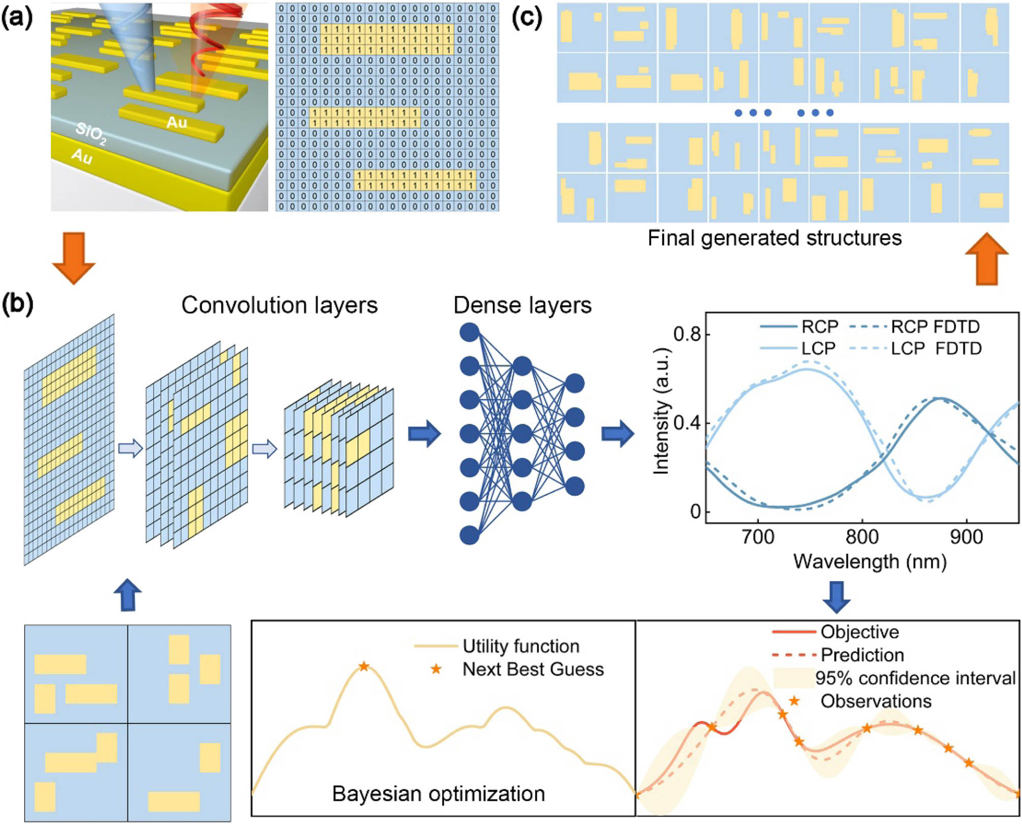
Figure 1.Schematic of the self-designed platform Bayesian optimization-net (BO-Net). (a) Left: the schematic of the self-designed waveplate, consisting of a metal-insulator-metal (MIM) unit cell. Right: the binary matrix parameterization. The shape of the top nanostructures is described by a
Based on our platform, the BO-Net strategy is utilized to retrieve optimal nanostructures [28], which can provide desired polarization conversion functionality with high efficiency. As a data-driven optimization strategy, an initial dataset, including structure parameters and Jones matrices, needs to be prepared in the beginning. Thus, 4000 samples are generated randomly through the “needle drop” approach, which can balance the accessible pattern diversity and accuracy of the nanofabrication. Each unit cell consists of 4 Au bricks in random locations, defined by 2 sets of coordinates of each brick’s rectangular diagonal vertex ( min, min, max, max), and the minimum size of the structures is set to 30 nm. Thus, location parameters of 4 bricks in one unit cell span a 16-dimensional parameter space, described by a matrix. Then, the numerical simulation is performed to provide the corresponding reflection spectrum of -polarized light. The Jones matrix can be extracted from the simulation result, and the relation between an incident field and a reflected field can be described as
As an example of what could be done, we design and experimentally demonstrate efficient half-waveplates (HWPs) composed of arbitrary-shape nanostructures, which can convert the circular polarization state of light with a high polarization conversion efficiency (PCE). The PCE is defined by
As the starting point of the DNN, the structure matrix (a matrix) and spectrum of randomly generated samples constitute the initial dataset, which is divided into 3 groups: 80% for training, 10% for validation, and 10% for testing. Training data are used to train a functionalized deep neural network for developing a relation between the structure geometry and its optical response, validation data are used to select the best model parameters, and the testing data are used to evaluate the generalization ability of the model. The upper part of Fig. 1(b) illustrates the DNN architecture, which includes two components: convolution layers and dense layers. Convolution layers aim to extract geometric features of the structures, and dense layers are devoted to mapping these features to reflection spectra. The optimization algorithm Adam (adaptive moment estimation) with the learning rate of is utilized to minimize the loss function, which is defined as the mean square error (MSE) between the output spectrum of FDTD simulations and DNNs. After 500 epochs of training, the mean square error of the obtained reflection spectra is on the training set and on the validation/testing set, which implies fairly high accuracy of the results from DNNs. Compared with conventional numerical methods, DNNs can predict the characteristic reflection spectrum through parallel tensor calculations without solving Maxwell’s equations, thus greatly shortening computation time and reducing the consumption of computational resources. Therefore, the well-trained network can take the place of FDTD methods to provide rapid predictions of reflection spectra that can be further employed in BO (see Appendix A).
The desired structure can be readily obtained with an objective function mapping structure matrix to the corresponding PCE averaged by wavelength. Nevertheless, the objective function is unavailable due to the enormous dimension () of parametrized design space. Therefore, we simplify the design space to a 16-dimensional parameter space spanned by four sets of geometrical parameters of nanostructures. BO is performed iteratively to approximate the objective function with an input size of 16 and to reinforce DNNs to search for the optimal structure with a higher PCE. As shown in the lower part of Fig. 1(b), the optical response of the given nanostructures, which is predicted by DNNs, accompanied with their structure parameters, which are described by a matrix, serves as an input of BO in one generation. Then, the overall input, up to the current generation, constitutes observations of the objective function and can be further utilized to approximate with a 95% confidence interval through Gaussian processes. The utility function is the upper bound of the confidence interval, and local maxima of this function yield recommended structures for the next generation, which is termed the “next best guess.” These structures and their optical response not only serve as an updated input for BO but also are recorded in a database for advanced design. This process is iterated continuously and improves the overall PCE of the whole database until the model converges. Eventually, a vast number of different nanostructures with high PCE [Fig. 1(c)] can be generated straightway via our well-trained model (see Appendix A).
As a cornerstone of our BO-Net, the accuracy and efficiency of DNNs are examined by calculating the reflection spectrum of a given nanostructure under the LCP planewave, with FDTD-simulated results presented for comparison. The DNN-calculated intensity of LCP, RCP, and total reflected light is plotted in Fig. 2(a), together with FDTD-simulated results. The excellent agreement between the DNN result (solid line) and the FDTD result (dashed line) demonstrates that the reflection spectrum can be obtained via the DNN model with convincing accuracy. Furthermore, the powerful parallel computing capability of DNNs gives rise to an unprecedented computing speed, which is over four orders of magnitude higher than that of the FDTD method. Consequently, the optimization process can be greatly accelerated by using DNNs, accompanied with a declined consumption of computational resources.
![]()
Figure 2.Variation of the polarization conversion efficiency (PCE) during the optimization process. (a) The reflection spectrum of a given nanostructure for the left-handed circularly polarized (LCP) planewave, calculated by DNNs (solid lines) and FDTD (dashed lines). The inset displays the geometric morphology of the corresponding nanostructure. (b) The maximum of the PCE as a function of generations. The PCE (averaged by wavelength) of each nanostructure generated during the optimization process is recorded as a function of generations (the number of iterations). The inset shows the five-number (the minimum, first quartile, median, third quartile, and the maximum) summary of the PCE data in the first 5 generations. The vertical line through the box indicates the median, the whiskers from each quartile indicate the minimum or the maximum, and the box indicates the value range of 50% PCE distribution. (c) The PCR spectrum of the representative nanostructures selected from the first 9 generations, labeled from G1 to G9. The side panel displays the corresponding geometric morphology of G1–G9, in the order from bottom to top.
Based on this framework, our design method is employed to maximize the circular PCE of the HWPs by automatic elaborate design of the nanostructures. The working wavelength is set from 650 to 950 nm to avoid the Au absorption band. As depicted earlier, 4000 random structures are generated, and their reflection spectra are forecasted through DNNs in order to create
In Fig. 2(c), geometries of the representative nanostructure generated by BO in the first 9 generations are depicted together with their corresponding PCE spectrum. As anticipated, the PCE is fairly low for the first generation. Then, the diversity of geometry increases with exploration strategies of BO for searching structures with a higher PCE. As the optimization keeps processing, the PCE is progressively enhanced, and some common features in the geometry of nanostructures emerge gradually, such as the aspect ratio and the filling factor. In essence, this variation trend indicates that our method can extract valuable information from the existing data and develop a specialized inference model for estimating and evaluating the PCE of given nanostructures.
3. FABRICATION AND MEASUREMENTS
We implement practical HWPs for polarization state control according to the results of the aforementioned workflow. First, to demonstrate the reliability and accuracy of our optimization process, HWPs that consisted of selective nanostructures from different generations (labeled as stru1, stru2, stru3, stru4, and stru5 in order of increase in generations) were fabricated with a standard electron beam lithography (EBL) process followed by a lift-off process (see Appendix D). Figure 3(a) displays scanning electron microscope (SEM) images (FEI Quanta 450 FEG) of the HWP unit cell with a 45°-tilted view. The reflection spectrum of each sample under normally incident LCP light was measured in a reflected dark-field microscope (HSI V3, CytoViva Co.) with a detection wavelength that ranged from 650 to 950 nm and was normalized by the substrate reflection spectrum (see Appendix D). As expected, there is a gradual rise in the PCE from stru1 to stru5 [Fig. 3(a)], signifying an increase in the PCE through the iterative optimization process.
![]()
Figure 3.Reflection measurement results and the characterization of the optimized database. (a) The measured PCE spectra of the representative nanostructures from different generations in the half-waveplates (HWPs) design process, labeled as stru1, stru2, stru3, stru4, and stru5 in order of increase in the generations. Side panel: SEM images of the corresponding nanostructures. (b), (c) The measured polarization conversion ratio (PCR) spectra of eight randomly selected unit cells of the HWPs (b) and QWPs (c) from the optimized database. Side panel: SEM images of the corresponding structures. (d) The simulated phase shift of the reflected light, which is introduced by the nanostructures in the optimized database. Each pixel corresponds to a nanostructure in the optimized database, the
Then, four representative practical HWPs, comprising nanostructures randomly selected from the optimized database, were fabricated and tested by the same scheme. Measured results are shown in Fig. 3(b), where the side panel displays SEM images of corresponding nanostructures. A striking feature is that the measured PCR of each nanostructure approaches 98% and stays around 90% in a broad wavelength range. Numerical simulations show a good agreement with experimental results as the PCR of each structure keeps close to 100% from 650 to 950 nm (see Appendix B). The discrepancy may be ascribed to the fabrication error and imperfect performance of optical components, especially the broadband quarter-waveplates (QWPs) and rotation errors during the measurement, thereby resulting in non-ideal circularly polarized incident light.
Our method can be directly generalized to the design of arbitrary wave plates, thereby enabling the customization of polarization states of reflected light. For the incident light, which can be expressed by the normalized Jones vector , the reflected light can be obtained from Eq. (1), including the Jones matrix. The initial training set in the DNNs only needs to be calculated once because the Jones matrix is constant for a certain unit cell, which can greatly reduce the time consumption of the optimization process. Therefore, to design desired functional wave plates, we only need to optimize a certain PCE based on the existing training dataset. As proof, we can get a large number of QWPs by our method, which can completely convert the incident linearly polarized light to RCP light. To impart the desired polarization response, we employ the DNNs to get the relation between the PCE and structure geometry and utilize BO to optimize the structure for a higher PCE.
Four representative unit cells are selected from the optimized result, which have PCEs higher than 80% and PCRs close to 100%, as demonstrated by FDTD simulation. The SEM images of the fabricated samples and measured reflection spectra are shown in Fig. 3(c), where the highest PCR approaches 90%. It is worth noting that, albeit the bandwidth of optimized nanostructures is designed to be 300 nm, they possess good polarization conversion capability in a wider wavelength range from 650 to 1500 nm. Moreover, to verify the universality of our method, we designed eight different polarization conversion devices to deal with other polarizations. Within the designed bandwidth, the PCR is close to 100%, showing the excellent performance. Overall, these results indicate that our self-designed wave plates from the optimized database possess an excellent capability of broadband polarization state control. More information is shown in Appendix B.
Moreover, we extracted the phase shift introduced by nanostructures within the optimized database by calculating the phase of reflected RCP light [Fig. 3(d)]. Each pixel represents a certain structure element in the optimized database, and the color represents the magnitude of its CE at the corresponding wavelength. We find that the phase shift can almost cover a cycle from 0 to over the whole working band (see Appendix C). More intriguingly, this phase shift is determined by the resonant interaction between the incident light and nanostructures, which is fundamentally different from the Pancharatnam–Berry (PB) phase. As a consequence, the resonant phase and PB phase introduced by the nanostructure in our database can be tuned independently, which can be applied to achieve full and independent control of polarization channels [42]. In a similar vein, the great potential of our nanostructures in applications of achromatic devices is illustrated by the dispersion relation of reflected RCP light [Fig. 3(e)]. Each dot represents a structure element in the overall database, which is developed during the whole optimization process, with the coordinates and color determined by the group delay, the PCE, and the coefficient of determination (). The distribution of data points shows that the group delay of the reflected light spans from 0 to 10 fs, and the maximum PCE at each group delay mostly stays above 40%. This result indicates that our nanostructures generated via deep neural networks can be applied for constructing efficient broadband achromatic optical devices [38].
4. DESIGN AND SIMULATION RESULTS OF ACHROMATIC METALENS
To demonstrate the versatility of the optimized database for constructing functional optical devices, an achromatic metalens was designed with a numerical demo. Figures 4(a) and 4(b) show the geometry of the metalens, which works at with a 200 nm bandwidth and possesses a diameter and focal length .
![]()
Figure 4.Designed achromatic metalens with a polarization conversion function. (a) The schematic of an achromatic metalens designed at the center wavelength of 800 nm with a bandwidth of 200 nm. (b) The magnified view of the metallic nanostructures of a region of the metalens. (c) The required and realized relative group delay from the center to the edge of the achromatic metalens. (d) The realized phase profile (dot lines) and the ideal phase profile (solid lines) at wavelengths of 700 nm, 800 nm, and 900 nm. (e) The simulated intensity distributions in the linear scale of the different wavelengths. The white dashed lines pass through the center of the focal spots in the case of
For an achromatic metalens accompanied with a polarization conversion function, a high PCE is required to get a feasible efficiency, which can be done with the optimized database. Besides, the group delay and phase of each element follows:
With selected elements located at fixed positions, we modulate their relative phase at the center wavelength by rotation around its center, i.e., adjusting their PB phase. Considering Eq. (A1) and the phase relation between the incident LCP light and reflected RCP light, the rotation angle of each element at center frequency follows
The realized relative phase by rotated elements at different wavelengths is plotted as dotted lines in Fig. 4(d), with the relative phase of a perfect achromatic metalens plotted as solid lines. The realized relative phase coincides with the ideal relative phase profile at the center wavelength 800 nm and shows a good agreement at 700 and 900 nm wavelength.
Furthermore, we performed a numerical simulation of the performance of our designed achromatic metalens using FDTD. The focal lengths at different wavelengths were obtained by acquiring the intensity profile of reflected RCP light along the propagating direction (-axis), as shown in Fig. 4(e). The white dashed line indicates the focal plane corresponding to an illumination wavelength of 800 nm. Due to the limitation of computation resources, the size of the designed metalens is finite (). Therefore, there is only a small number of elements to map the change over the lens radius, which results in a shorter focal length in simulation than the designed one.
In Fig. 4(f), we also acquired the focal spot profile at the focal plane corresponding to an illumination wavelength of 800 nm [white dashed line in Fig. 4(e)]. The focal spots at different wavelengths are diffraction-limited and maintain their profile for the entire working wavelength range from 700 to 900 nm. This demo of achromatic metalens demonstrates that a large number of different structures with high PCE in the optimized database can be easily transferred to the design of complex functional devices such as achromatic metalenses.
5. CATHODOLUMINESCENCE MICROSCOPY AND THEORETICAL ANALYSIS
To elucidate the underlying physical basis for the broadband polarization state conversion of designed wave plates, we further imaged the polarization-dependent electromagnetic modes that hide in the optical near-field of the nanostructure by using CP-resolved CL microscopy (Gatan MonoCL Plus [43,44]). More information is shown in Appendix D. According to the reciprocity theorem between electron beam excitation and plane wave illumination [45], the CP-resolved CL emission is generally related to the component of the electric field under CP light illumination. Therefore, the distribution of the near-field electromagnetic modes can be well imitated by the CL mapping, which is acquired by scanning the sample with a focused electron beam and recording corresponding CL emissions. Figures 5(a) and 5(b) display a series of bandpass LCP CL images of fabricated HWPs and QWPs (2 HWPs: struB and struD; 2 QWPs: struIII and struIV) with a center wavelength at 510 and 794 nm. At 794 nm, the distribution of CL hot-spots can be clearly distinguished and shows a chiral feature at corners and edges, which reveals a chiral electromagnetic mode caused by a strong polarization-dependent interaction between nanostructures and incident light. Conversely, the intensity of the CL emission is homogeneously distributed on Au nanostructures at 510 nm, and the overall intensity is much lower than that at 794 nm, thus indicating a much weaker interaction between nanostructures and incident light. This result, which has a good agreement with the simulated chiral near-field distribution, suggests that the strong polarization-dependent interaction and the chiral optical near field can be the mutual origin of the strong capability of polarization state control that our nanostructures exhibit from 650 to 950 nm (see Appendix B).
![]()
Figure 5.Bandpass left-handed circularly polarized (LCP) cathodoluminescence (CL) images and reflection matrix. (a), (b) Bandpass LCP CL images (
In order to analyze the detail of high PCE theoretically, the polarization state of output light can be depicted by the Stokes parameter S3, which is defined as the normalized intensity difference between RCP and LCP components. In the circumstance of the complete transformation of circular polarization of perfect HWPs, the reflection matrix in Eq. (1) has to satisfy the following conditions:
To get a perfect QWP with a 45° major axis (with respect to the -axis), the reflection matrix has to satisfy
To compare with the ideal condition, the reflection matrix of 4 representative nanostructures (2 HWPs and 2 QWPs) and S3 are both calculated via numerical simulations, and the amplitude profile of each matrix element and S3 are illustrated in Figs. 5(c) and 5(d). For the HWPs, it is observed that the amplitude of and stays around 1 over the working band, according to Eq. (1), indicating that the nanostructure can preserve the linear polarization without dissipation and deflection. Additionally, S3 varies abruptly from to 1 at around 600 nm and keeps uniform after 650 nm, confirming an excellent efficiency of our HWPs for the polarization state transformation. As for the QWPs, S3 equals 0 from 450 to 540 nm since the interaction between the incident light and nanostructures is extremely weak, and the incident polarization is preserved. Nevertheless, S3 changes to after 650 nm, ensuring a nearly perfect RCP light we can get.
The phases of the dominant matrix elements as a function of wavelengths are shown in Figs. 5(e) and 5(f), which are close to 0 from 450 to 510 nm, implying a negligible interaction between the nanostructure and incident light. However, they become non-zero in a wavelength range from 650 to 950 nm, and the phase difference between two matrix elements is approximately equal to (HWPs) and (QWPs), satisfying the condition in Eqs. (4) and (5). It is worth noting that the sharp dip of the amplitude profile and the dramatical oscillation of the phase between 520 and 650 nm result from the strong resonant interaction between the metallic nanostructure and incident light. These facts demonstrate that the reflection matrix of the nanostructure is consistent with that of the perfect HWPs and the QWPs, leading to a complete transformation of polarization states.
Accordingly, our analysis provides important insights into the strong polarization-dependent interaction between the incident radiation filed and metallic nanostructures, which is an integral aspect of polarization state manipulation. It is also important to point out here that although our BO-Net presets no physical rule as a guideline for the optimization process, it explores and learns characteristic features of structures with a high PCE from the randomly generated database independently. Hence, based on hidden common features, it can generate a larger number of desired nanostructures with a great physical interpretability, which can be generally analyzed by the Jones matrix. Due to the absence of specific guidelines in the optimization process, the physical mechanism of the great polarization-state-control capability can be various in detail among generated nanostructures, which may expand scopes in the realm of optical metamaterials and nanophotonics.
6. CONCLUSION
In conclusion, we have utilized BO-Net to design and experimentally demonstrated arbitrary wave plates with excellent capability to control the polarization state of light. The reflection measurement confirms that the fabricated HWPs and QWPs allow for a broadband polarization ratio over 90% across a 300-nm-wide bandwidth (650–950 nm). Through the CL microscopy with deep-subwavelength resolution, the underlying physics of the polarization-dependent interaction between the nanostructure and incident light emerges, which is also theoretically analyzed with the Jones matrix. Our proposed method and structures for polarization state control provide a platform to shed light on the polarization-dependent interaction between light and materials and to inspire the design of nanophotonic devices. Notably, due to the powerful parallel computing capability, the presented BO-Net can generate plentiful desired nanostructures while using limited computing resources, which can be applied to develop a practical database for advanced design. The phase shift of structures in our database can be combined with other phase-addressing mechanisms, opening an avenue for the multidimensional manipulation of light and multiplexed broadband optical devices. On a more fundamental level, compared to the conventional design strategies based on preset physical rules, our method exhibits a higher efficiency and degree of freedom, which can implement previously inaccessible complicated tasks. Therefore, we envision that this method will become an efficient tool for optimization in several scientific areas, including optics, acoustics, electronics, and engineering physics.
APPENDIX A: SELF-DESIGNED PLATFORM BO-NET
The architecture of the deep neural network is schematically shown in Fig.
![]()
Figure 6.Schematic diagram of the deep neural network.
![]()
Figure 7.Loss evolution during the training process on both the training set and the validation set. (a), (b) The loss evolution of the LCP and the RCP spectrum for the half-wave plates (HWPs) design. (c), (d) The loss evolution of the LCP and the RCP spectrum for the quarter-wave plates (QWPs) design.
![]()
Figure 8.Variation of the PCE during the optimization process of the QWPs. The PCE (averaged by wavelength) of each nanostructure generated during the optimization process is recorded as a function of generations (the number of iterations). The inset shows the five-number (the minimum, first quartile, median, third quartile, and the maximum) summary of the PCE data in the first 5 generations. The vertical line through the box indicates the median, the whiskers from each quartile indicate the minimum or the maximum, and the box indicates the value range of 50% PCE distribution.
APPENDIX B: NUMERICAL SIMULATION RESULTS
In order to evaluate the performance of optimized nanostructures, we show PCR and PCE spectra of some QWPs (Fig.
![]()
Figure 9.Examples of the optimized nanostructures in our database. (a)–(f) The reflection spectrum of a given nanostructure (inset) under a normally incident LCP planewave, calculated by the DNNs (solid lines) and the FDTD simulations (dashed lines). (a)–(d) These nanostructures are fabricated and measured, and the results are shown in the main text.
![]()
Figure 10.Examples of the optimized nanostructures in our database. The reflection spectrum of a given nanostructure (inset) under a normally incident
![]()
Figure 11.Simulated broadband spectrum of the optimized nanostructures in our database. (a), (b) The reflection spectrum of a given HWP (inset) under a normally incident LCP planewave, calculated by FDTD simulations from 450 to 2000 nm. (c), (d) The reflection of a given QWP (inset) under a normally incident
![]()
Figure 12.(a)–(h) Reflection spectra of a given optimized nanostructure (as shown in the insets) under a normally incident polarized planewave, calculated by the FDTD simulations. The In (short for input) indicates the Jones vector of the incident polarized planewave, and the Out (short for output) indicates the Jones vector of the objective reflected polarized planewave. The PCE and the PCR are profiled by red and blue solid lines, respectively.
![]()
Figure 13.Simulated electric field distribution of the metallic nanostructure under a normally incident LCP planewave with a wavelength at 510 nm and 794 nm, respectively. Corresponding experimental results are shown in the main text.
APPENDIX C: ACHROMATIC DEVICES
Consider the achromatic metalens, the relative phase provided by the metalens elements with respect to the center follows
![]()
Figure 14.Schematic of an achromatic metalens. The metalens is designed to provide spatially dependent group delays such that wave packets from different locations arrive simultaneously at the focus. The yellow line shows the spherical wavefront.
![]()
Figure 15.Group delay of the metallic nanostructure. The group delay (
![]()
Figure 16.Examples of the self-designed HWPs for different wavelengths and the phase shift with a relatively high PCE.
APPENDIX D: EXPERIMENTS
The samples were fabricated by using the standard thin-film deposition, electron-beam lithography (EBL), and lift-off techniques. First, a 2-nm-Ti layer and a 50-nm-Au layer were deposited on a silicon substrate through electron beam evaporation. Then, a 100-nm-thick spacer layer was developed with chemical vapor deposition. After spin-coating positive resist (Mirco Chem PMMA A2 950), designed structures were patterned in the scanning electron microscope (SEM, FEI Quanta 450 FEG) under the control of the Nano Pattern Generation System (NPGS) module. Next, the 2 nm Ti as the adhesion layer and 40 nm Au were deposited by electron beam evaporator (DE400DHL, DE Technology). Finally, metallic nanostructures were formed by the lift-off process.
All of the spectra were acquired by a commercial dark-field microscope (HSI V3, CytoViva Co.) in addition to linear polarizers and quarter-wave plates in the collection optical path for distinguishing LCP or RCP light. Under illumination of normally incident -polarized light, the reflection spectra of nanostructures were calibrated and normalized by the substrate reflection spectrum.
CL measurements were performed by a CL detection system (Gatan MonoCL4 Plus) mounted on an SEM (FEI Quanta 450 FEG) [
![]()
Figure 17.Schematic of the CL microscopy. The emissions passing through the optical path were acquired by a highly-sensitive photomultiplier tube (PMT) (HSPMT, 160–930 nm). Locating the fast axis of the quarter-wave plate by
References
[13] P. St. J. Russell. Not just saying no. Nature, 381, 290(1996).
[19] N. Yu, F. Capasso. Flat optics with designer metasurfaces. Nat. Mater., 13, 139-150(2014).
[20] S. Jahani, Z. Jacob. All-dielectric metamaterials. Nat. Nanotechnol., 11, 23-36(2016).
[34] S. Kim, P. Y. Lu, C. Loh, J. Smith, J. Snoek, M. Soljačić. Deep learning for Bayesian optimization of scientific problems with high-dimensional structure. arXiv(2022).
[47] E. Brochu, V. M. Cora, N. de Freitas. A tutorial on Bayesian optimization of expensive cost functions, with application to active user modeling and hierarchical reinforcement learning. arXiv(2010).

Set citation alerts for the article
Please enter your email address
© Copyright 2018-2021 | Chinese Laser Press. All Rights Reserved 沪ICP备15018463号-20