• Journal of Semiconductors
  • Vol. 40, Issue 8, 081508 (2019)
Xiaoxi Li1、2, Baojuan Dong1、2, Xingdan Sun1、2, Hanwen Wang1、2, Teng Yang1、2, Guoqiang Yu3、4, and Zheng Vitto Han1、2
Author Affiliations
  • 1Shenyang National Laboratory for Materials Science, Institute of Metal Research, Chinese Academy of Sciences, Shenyang 110016, China
  • 2School of Material Science and Engineering, University of Science and Technology of China, Hefei 230026, China
  • 3Beijing National Laboratory for Condensed Matter Physics, Institute of Physics, Chinese Academy of Sciences, Beijing 100190, China
  • 4Center of Materials Science and Optoelectronics Engineering, University of Chinese Academy of Sciences, Beijing 100049, China
  • show less
    DOI: 10.1088/1674-4926/40/8/081508 Cite this Article
    Xiaoxi Li, Baojuan Dong, Xingdan Sun, Hanwen Wang, Teng Yang, Guoqiang Yu, Zheng Vitto Han. Perspectives on exfoliated two-dimensional spintronics[J]. Journal of Semiconductors, 2019, 40(8): 081508 Copy Citation Text show less
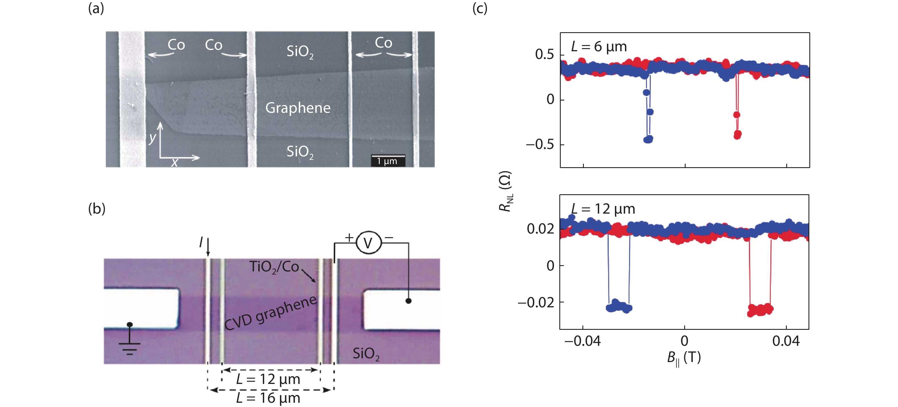
    (Color online) (a, b) Typical spin valve devices made of graphene[33, 34]. (c) The performance of non-local magneto-resistance for CVD graphene spin valve with different channel lengths[34].
    Fig. 1. (Color online) (a, b) Typical spin valve devices made of graphene[33, 34]. (c) The performance of non-local magneto-resistance for CVD graphene spin valve with different channel lengths[34].
    (Color online) (a, b) Schematics of configurations for 2D spin valve devices, and (c) 2D spin filter tunnel junction (sf-TJ). (d–f) The first spin valve demonstrated using 2D vdW magnetic (Fe-doped TaS2) materials[94].
    Fig. 2. (Color online) (a, b) Schematics of configurations for 2D spin valve devices, and (c) 2D spin filter tunnel junction (sf-TJ). (d–f) The first spin valve demonstrated using 2D vdW magnetic (Fe-doped TaS2) materials[94].
    (Color online) (a) Schematics of CrI3 sf-TJ[96]. (b–d) Optical images of several iterations of vdW 2D sf-TJ devices since 2017[96, 99, 106]. Notice that all of them have very small junction area possibly to reduce the number of magnetic domains. (e, f) The magneto-tunneling current and spin-filtered magnetoresistance for a four-layered CrI3 sf-TJ device[96].
    Fig. 3. (Color online) (a) Schematics of CrI3 sf-TJ[96]. (b–d) Optical images of several iterations of vdW 2D sf-TJ devices since 2017[96, 99, 106]. Notice that all of them have very small junction area possibly to reduce the number of magnetic domains. (e, f) The magneto-tunneling current and spin-filtered magnetoresistance for a four-layered CrI3 sf-TJ device[96].
    (Color online) Optical image of several versions of spin-FETs based on magnetic vdW materials (a) semiconducting CrSiTe3[62], (b) semiconducting Cr2Ge2Te6[110], (c) h-BN encapsulated Cr2Ge2Te6 (red and black dashed lines label the edge of Cr2Ge2Te6 and graphene electrodes, respectively)[15], and (d) Al2O3-assisted exfoliated 4-layered metallic Fe3GeTe2[17], respectively. Scale bars in (c) and (d) are 10 and 100 μm, respectively. (e) Schematic of the tunable Fermi level and simplified spin-polarized band structure of the vdW intrinsic magnetic semiconductor[15]. (f, g) Gate tuned magnetic hysteresis loops and gate-tuned I–V curves of the few-layered Cr2Ge2Te6 planar FET device[15]. (h, i) Longitudinal conductivity and Curie temperature of the Fe3GeTe2 planar FET as a function of ion liquid gate[17]. (j) The anomalous Hall curves of the ionic-gated Fe3GeTe2 planar FET at different temperatures[17].
    Fig. 4. (Color online) Optical image of several versions of spin-FETs based on magnetic vdW materials (a) semiconducting CrSiTe3[62], (b) semiconducting Cr2Ge2Te6[110], (c) h-BN encapsulated Cr2Ge2Te6 (red and black dashed lines label the edge of Cr2Ge2Te6 and graphene electrodes, respectively)[15], and (d) Al2O3-assisted exfoliated 4-layered metallic Fe3GeTe2[17], respectively. Scale bars in (c) and (d) are 10 and 100 μm, respectively. (e) Schematic of the tunable Fermi level and simplified spin-polarized band structure of the vdW intrinsic magnetic semiconductor[15]. (f, g) Gate tuned magnetic hysteresis loops and gate-tuned IV curves of the few-layered Cr2Ge2Te6 planar FET device[15]. (h, i) Longitudinal conductivity and Curie temperature of the Fe3GeTe2 planar FET as a function of ion liquid gate[17]. (j) The anomalous Hall curves of the ionic-gated Fe3GeTe2 planar FET at different temperatures[17].
    (Color online) (a, b) Schematic and optical image of a typical Pt/FGT device[124]. (c) Hall resistivity recorded as a function of current flowing in the 2D vdW heterostructure device. A hysteresis loop can be seen, demonstrating the current-driven magnetic switch of the magnetizations in the FGT layer[124]. (d) Switching current as a function of externally applied in-plane magnetic fields at different temperatures[124]. (e) Schematic structure of Pt/FGT device[125]. (f) Anomalous Hall effect curve of the Pt/FGT device[125]. (g) Current-induced magnetic switch at different external magnetic fields[125].
    Fig. 5. (Color online) (a, b) Schematic and optical image of a typical Pt/FGT device[124]. (c) Hall resistivity recorded as a function of current flowing in the 2D vdW heterostructure device. A hysteresis loop can be seen, demonstrating the current-driven magnetic switch of the magnetizations in the FGT layer[124]. (d) Switching current as a function of externally applied in-plane magnetic fields at different temperatures[124]. (e) Schematic structure of Pt/FGT device[125]. (f) Anomalous Hall effect curve of the Pt/FGT device[125]. (g) Current-induced magnetic switch at different external magnetic fields[125].
    (Color online) Illustration of different nanostructures for vdW spintronics.
    Fig. 6. (Color online) Illustration of different nanostructures for vdW spintronics.
    (Color online) A roadmap for the exfoliated spintronics.
    Fig. 7. (Color online) A roadmap for the exfoliated spintronics.
    MaterialBandgapMagnetic orderingsWay to getMeasurement techniquesExchange interactions Critical temperature TC/TNTunability
    CrI3[13, 14, 20, 63]1.2 eVIntralayer/FM Interlayer/AFM FM/bulkExfoliatedMagneto-optic Kerr effect (MOKE)Ising/direct Double-exchange/ super-exchange 64 K/bulk 45 1LThickness Gate/ionic liquid electric field
    CrBr3[2123, 46]2.1 eV/bulkFM/bulk FM/2DHQ graphene provided/bulk Exfoliated/1LMagnetic circular dichroism (MCD)Heisenberg/direct35 K/bulk 37 K/3L 36/2L 27/1L Not available (NA)
    CrCl3[24, 57, 64, 65]3.1 eV/bulkIntralayer/FM Interlayer/AFM AFM/bulkChemical vapor transport(CVT)/bulk Exfoliated/2LTunnelingXY/direct14 K/bulk 17 K/few-layer 16/2L Thickness
    Cr2Si2Te6[62, 6669]0.4 eV/direct-bulk 1.2 eV/indirect/bulkFMSelf-flux/bulk Exfoliated/2DHeisenberg/direct Double-exchange/ super-exchange 32 K/bulk 80 K/2D Thickness
    Cr2Ge2Te6[15, 19]0.45 eVFMExfoliatedMOKEHeisenberg/direct45 K(bulk)Gate/ionic liquid
    Fe3GeTe2[17]0FMA12O3 assisted exfoliated Anomalous Hall Effect (AHE)Ising/direct Itinerate/super-exchange 180 K/bulk 20 K/1L Thickness Ionic liquid
    FePS3[25, 70]1.5 eVAFMCVTRaman + DFTIsing/direct123 K/bulk 118 K/1L NA
    MnPS3[25, 26, 47]2.4 eVAFMCVT/bulk Exfoliated/2DPhysical property measurement systems (PPMS)/bulk RamanHeisenberg/direct78 K/bulkLiquid gating
    NiPS3[27, 71]1.6 eV/indirect >2.4 eV/direct AFMCVT/bulk Exfoliated/2LRamanXY/direct155 K/bulk 130 K/2L NA
    VSe2[17, 29]0FM/1L AFM/2L Paramagnetic/bulkMolecular beam epitaxy(MBE)MOKE AHENA>300 KThickness Electric field
    CrTe2[72]0FMOxidation of KCrTe2SquidItinerate/super-exchange310 K/bulkNA
    V5S8[30]0AFM/bulk FM/3.2 nmChemical Vapor Deposition (CVD)/10 nm Exfoliated/3.2 nmAHENA32 K/bulk 2 K/3.2 nm Thickness
    CrSe[31]NAFMCVDPPMSNA208 KNA
    Cr2S3[32]NAFMCVDPPMSNA120 KNA
    Table 1. A list of typical 2D vdW magnetic materials and their magnetic fingerprints.
    Xiaoxi Li, Baojuan Dong, Xingdan Sun, Hanwen Wang, Teng Yang, Guoqiang Yu, Zheng Vitto Han. Perspectives on exfoliated two-dimensional spintronics[J]. Journal of Semiconductors, 2019, 40(8): 081508
    Download Citation