
Xiaoxi Li, Baojuan Dong, Xingdan Sun, Hanwen Wang, Teng Yang, Guoqiang Yu, Zheng Vitto Han. Perspectives on exfoliated two-dimensional spintronics[J]. Journal of Semiconductors, 2019, 40(8): 081508
- Journal of Semiconductors
- Vol. 40, Issue 8, 081508 (2019)
Abstract
1. Introduction
In general, spintronics such as spin valves must involve in their structures multiple layers of magnetic thin films[
Liberating the degrees of freedom of lattice-matching as well as the demanding growth conditions had never been so facile until the day when graphene was exfoliated by simply using a scotch tape[
Magnetic vdW materials, by definition, are consisted of 2D layers with spontaneous spin polarization below their magnetic critical temperatures. A long-range spin ordering was long believed not to be available in 2D as predicted by the early theories based on the isotropic Heisenberg models[
Compared to their 3D counterparts, the advantages of magnetic 2D materials can be twofold. Firstly, 2D magnets can be seamlessly assembled with different rotational angles between the layers of different kinds, thus allowing band engineering through tunable moiré super lattices. Secondly, many of the 2D magnets can be implemented into in-plane field effect transistors, as they are semiconducting with Fermi levels gate tunable. It thus largely increases the opportunities for future spintronic applications, in terms of not only the variety of materials but also the emergent physical phenomena that arise from the novel 2D nanostructures. In this review, we will briefly describe the state-of-the-art spintronics based on 2D vdW materials and offer a new perspective by drawing a potential roadmap of vdW spintronics for the next decade.
2. The ‘pre-history’ of vdW magnets spintronics
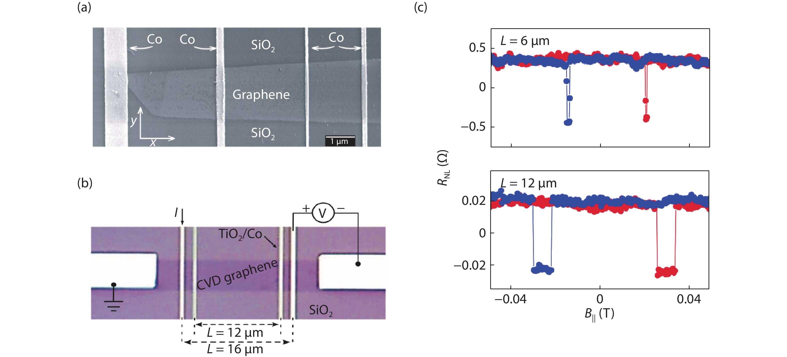
Many of the vdW materials are non-magnetic. However, even in the early days of the 2D materials research, spin-related phenomena have already attracted vast attentions. Indeed, spin injection from magnetic electrodes into non-magnetic substrates can work as an in-plane configuration of spin valves[
![]()
Figure 1.(Color online) (a, b) Typical spin valve devices made of graphene[
Except for direct spin injections, MoS2 was also found to be a candidate for spin manipulations in an optical manner due to the spin-valley locking in this specific type of 2D material[
As stated above, before the isolation of 2D intrinsic vdW magnetic materials, spin-related phenomena have been widely studied in a broad range of vdW materials, which can be categorized in the volume of the ‘pre-history’ of intrinsic vdW magnets.
3. Exfoliated intrinsic vdW magnets spintronics
2D vdW magnets are not at all new materials, while they were just for unknown reasons not quite exfoliated before 2017. Actually, the bulk forms of layered magnetic compounds have been well characterized in terms of crystallographic and spin structures[
To date, experimental examinations together with theoretical predictions show that most spin exchange interactions in the 3D scenario (including direct Ising and XY interactions, and other indirect interactions) can prevail down to the 2D limit[
The successful exfoliation of vdW magnets is just the beginning of the game, like every new topic in condensed matter physics — people have to find new physics, as well as new applications out of them. In the coming sections, we will discuss a couple of examples of such efforts.
4. Spin valves based on exfoliated vdW magnets
Spin valves have planar configurations as indicated in Section 1 and in Fig. 2(a), as well as vertical configurations that sometimes take the advantage of electron tunneling by sandwiching a tunneling insulator between two ferromagnetic (FM) layers, as shown in Fig. 2(b). This FM-insulator (I)-FM structure is well known as tunneling magnetoresistance (TMR)[
![]()
Figure 2.(Color online) (a, b) Schematics of configurations for 2D spin valve devices, and (c) 2D spin filter tunnel junction (sf-TJ). (d–f) The first spin valve demonstrated using 2D vdW magnetic (Fe-doped TaS2) materials[
The first attempt of the vertical spin valve using vdW magnetic materials was realized in 2015, with two pieces of few-layered Fe-doped TaS2 as the FM layers, while the tunnel layer was oxides formed naturally between their interface (Figs. 2(d) and 2(e)[
Magnetic vdW materials can be easily exfoliated on a desktop and assembled into spintronic devices, which are free of epitaxial technology and in principle can be mass-produced by means of chemical vapor deposition (CVD) etc. It thus opens up a totally new page and shall give a profound impact on the future of the spin-valve industries. Nevertheless, the experimentally-demonstrated spin valves are, so far, working far below room temperature. The transfer/stacking method is yet to be optimized for batch production, which will also be discussed from a broad perspective in the last section of this review.
5. vdW magnetic tunnel junctions
Besides the FM–I–FM configuration, metal–FM–metal configuration, which has the insulating FM sandwiched between two metals, has also been used as spintronic device, often referred to as spin filter tunnel junction (sf-TJ), as shown in Fig. 2(c). As given in Table 1, many of the vdW magnetic materials (including CrI3, CrBr3 and etc.) have semiconducting gaps, and usually are quite insulating at low temperature, thus providing a unique chance for the study of 2D vdW sf-TJs and related tunneling physics.
Indeed, several experiments have confirmed that multilayered-CrX3 (X = I, Br, Cl) sf-TJs have extremely large magnetoresistance up to ~ 106%[
In addition to the applications stated above, sf-TJs made of vdW magnetic tunnel layers can serve in a new kind of vertical spin-related field effect transistor. In this scenario, transparent few-layered graphene gate electrodes are often equipped within the structure illustrated in Fig. 3(a), in the sense that optical probe can penetrate the graphene gate without catching any parasitic magnetic signals but the ones from the vdW magnetic tunneling layer itself. During measurements, gate voltages can be seamlessly applied, pumping electron in and out of the band structure of the target vdW magnet and sequentially affecting the magnetic parameters including coercivity, Curie temperature, and etc.[
![]()
Figure 3.(Color online) (a) Schematics of CrI3 sf-TJ[
It is noteworthy that, so far, investigations on sf-TJs that utilize antiferromagnetic vdW layers as tunnel barrier remain scarce. To some extent, both sf-TJs (Fig. 2(c)) and TMRs (Fig. 2(b)) can be used as logic unit and magnetic sensors[
6. Planar vdW magnetic field effect transistors
Not quite similar to the sf-TJ with insulating vdW magnetic tunnel layer mentioned above, a real planar structure that mimics the famed metal-oxide field effect transistor (FET) can also be achieved in vdW magnets. This will require naturally a semiconducting channel, or at least a conducting channel whose electron density of states can be gate tuned, via electrostatic or liquid gate techniques.
A series of vdW materials Cr2M2Te6 (M = Si, Ge) compounds were reported to be intrinsic magnetic semiconductors, with reported band gaps varying in the range of 0.4–1.2 eV[
![]()
Figure 4.(Color online) Optical image of several versions of spin-FETs based on magnetic vdW materials (a) semiconducting CrSiTe3[
It was known that even conventional metallic thin Fe, Co films can manifest tunable magnetic parameters via ionic gating[
Up to now, studies on vdW magnetic semiconducting FETs are still on the go. There is plenty of room to improve the performances, including the working temperature, and the interface between FM and AFM vdW semiconductors, and etc.. While vdW FM semiconductors are of great interest for planar FETs, it is noteworthy that there is the family of vdW AFM semiconductors, which are also promising for planar FETs, as well as opto-electronic applications.
7. Current-driven switching of vdW magnets
About three decades after the theoretical predictions[
When interfaced with a magnetic layer, the SHE in the non-magnetic layer with large SOC can exert an orbit torque (SOT) on the magnetic layer that can switch the direction of magnetization, thus giving rise to a current-driven spin flip. During the switching process, a small external magnetic field colinear with the current is required[
Indeed, the reports in 2019 indicate that it is absolutely feasible to replace the conventional magnetic film with vdW ferromagnets in the SOT structures[
![]()
Figure 5.(Color online) (a, b) Schematic and optical image of a typical Pt/FGT device[
At the current stage, SOT devices using vdW magnets as a platform are still far from mature to meet the applicational standard, such as free of an external magnetic field, low critical switching current density, and etc. Apparently, room temperature operation is needed, and the SOC layers are so far still conventional metallic thin films. There is thus a long way to go to address the above points to push the vdW SOT devices towards real applications.
It is worth noting that spin Hall effects can be also observed via magneto-optical Kerr measurements as experimentally evidenced in semiconducting TMDs[
8. Other possibilities and an outlook of vdW spintronics
In the previous sections a couple of typical vdW spintronic devices such as spin valves, spin filter tunnel junctions, and planar spin FET have been introduced, and we now come to a brief discussion on several other configurations of spintronic devices using vdW magnets as a platform. In Fig. 6, a variety of nanostructures for vdW spintronics are illustrated. It can be seen that spin-related electronic devices can in principle be built via a mechanical stacking method, giving rise to possible applications such as 2D heterostructure of multi-ferroics, vdW magnetic recording, and topological magnetic states, etc. Up to now, the emerging phenomena in 2D vertical multi-ferroics as well as topological magnetic states in the vdW systems are attracting great interests. We now propose a roadmap for exfoliated spintronics, as indicated in Fig. 7. In short, depending on the development of vdW materials, the future trend of the vdW spintronics can be classified into fundamental- and application-oriented directions.
![]()
Figure 6.(Color online) Illustration of different nanostructures for vdW spintronics.
![]()
Figure 7.(Color online) A roadmap for the exfoliated spintronics.
For fundamental research, the future tasks will be looking for new emerging phenomena including topological magnetic states (Skyrmion[
For application research, the top priority will be to find room temperature vdW magnets. And the mission for future application shall include spin torque transfer (or spin Hall related) devices, spin diodes, spin valves, vdW magnetic semiconductors (as compared to the bulk diluted magnetic semiconductors[
Finally, we would like to recall the fact that, in principle, vdW magnetic materials are compatible with mass production processes such as CVD methods[
Acknowledgment
This work is supported by the National Key R&D Program of China (No. 2017YFA0206302), and is supported by the National Natural Science Foundation of China (Grants No. 51627801). G.Y. thanks the finical supports from the National Natural Science Foundation of China (Grants No. 11874409). T. Yang acknowledges supports from the Major Program of Aerospace Advanced Manufacturing Technology Research Foundation NSFC and CASC, China (No. U1537204).
References
[1] P M Tedrow, R Meservey. Spin polarization of electrons tunneling from films of Fe, Co, Ni, and Gd. Phys Rev B, 7, 318(1973).
[2] M Jullière. Tunneling between ferromagnetic films. Phys Lett A, 54, 225(1975).
[3] M Johnson, R H Silsbee. Interfacial charge-spin coupling: Injection and detection of spin magnetization in metals. Phys Rev Lett, 55, 1790(1985).
[4] M Baibich, J M Broto, A Fert et al. Magnetoresistance of (001)Fe/(001)Cr magnetic superlattices. Phys Rev Lett, 61, 2472(1988).
[5] G Binasch, P Grünberg, F Saurenbach et al. Enhanced magnetoresistance in layered magnetic structures with antiferromagnetic interlayer exchange. Phys Rev B, 39, 4828(1989).
[6] S Datta, B Das. Electronic analog of the electro-optic modulator. Appl Phys Lett, 56, 665(1990).
[7] B Dieny, V S Speriosu, S Metin et al. Magnetotransport properties of magnetically soft spin-valve structures. J Appl Phys, 69, 4774(1991).
[8] J S Moodera, L R Kinder, T M Wong et al. Large magnetoresistance at room temperature in ferromagnetic thin film tunnel junctions. Phys Rev Lett, 74, 3273(1995).
[9] E I Rashba. Properties of semiconductors with an extremum loop. I. Cyclotron and combinational resonance in a magnetic field perpendicular to the plane of the loop. Soviet Phys Solid State, 2, 1109(1960).
[10] K S Novoselov, A K Geim, S V Morozov et al. Electric field effect in atomically thin carbon films. Science, 306, 666(2004).
[11] M Nicolas, G Marco, S Philippe et al. Two-dimensional materials from high-throughput computational exfoliation of experimentally known compounds. Nat Nanotechnol, 13, 246(2018).
[12] K F Mak, C Lee, J Hone et al. Atomically thin MoS2: a new direct-gap semiconductor. Phys Rev Lett, 105, 136805(2010).
[13] B Huang, G Clark, E Navarro-Moratalla et al. Layer-dependent ferromagnetism in a van der Waals crystal down to the monolayer limit. Nature, 546, 270(2017).
[14] B Huang, G Clark, D R Klein et al. Electrical control of 2D magnetism in bilayer CrI3. Nat Nanotechnol, 13, 544(2018).
[15] Z Wang, T Zhang, M Ding et al. Electric-field control of magnetism in a few-layered van der Waals ferromagnetic semiconductor. Nat Nanotechnol, 13, 554(2018).
[16] N D Mermin, H Wagner. Absence of derromagnetism or antiferromagnetism in one- or two-dimensional isotropic Heisenberg models. Phys Rev Lett, 17, 1133(1966).
[17] Y J Deng, Y J Yu, Y C Song et al. Gate-tunable room-temperature ferromagnetism in two-dimensional Fe3GeTe2. Nature, 563, 94(2018).
[18] Z Y Fei, B Huang, P Malinowski et al. Two-dimensional itinerant ferromagnetism in atomically thin Fe3GeTe2. Nat Mater, 17, 778(2018).
[19] C Gong, L Li, Z L Li et al. Discovery of intrinsic ferromagnetism in two-dimensional van der Waals crystals. Nature, 546, 265(2017).
[20] D Zhong, K L Seyler, X Y Linpeng et al. Van der Waals engineering of ferromagnetic semiconductor heterostructures for spin and valleytronics. Sci Adv, 3, 5(2017).
[21] D Ghazaryan, M T Greenaway, Z Wang et al. Magnon-assisted tunnelling in van der Waals heterostructures based on CrBr3. Nat Electron, 1, 344(2018).
[22] E J Samuelsen, R Silberglitt, G Shirane et al. Spin waves in ferromagnetic CrBr3 studied by inelastic neutron scattering. Phys Rev B, 3, 157(1971).
[23] H H Kim, B W Yang, S W Li et al. Evolution of interlayer and intralayer magnetism in three atomically thin chromium trihalides. PNAS, 116, 11131(2019).
[24] X H Cai, T C Song, N P Wilson et al. Atomically thin CrCl3: an in-plane layered antiferromagnetic insulator. Nano Lett, 19, 3993(2019).
[25] Z U Rehman, Z Muhammad, O A Moses et al. Magnetic isotropy/anisotropy in layered metal phosphorous trichalcogenide MPS3 (M = Mn, Fe) single crystals. Micromachines, 9, 292(2018).
[26] G Long, T Zhang, X B Cai et al. Isolation and characterization of few-layer manganese thiophosphite. ACS Nano, 11, 11330(2017).
[27] K Kim, S Y Lim, J U Lee et al. Suppression of magnetic ordering in XXZ-type antiferromagnetic monolayer NiPS3. Nat Commun, 10, 345(2019).
[28] M Bonilla, S Kolekar, Y J Ma et al. Strong room-temperature ferromagnetism in VSe2 monolayers on van der Waals substrates. Nat Nanotechnol, 13, 289(2018).
[29] S J Gong, C Gong, Y Y Sun et al. Electrically induced 2D half-metallic antiferromagnets and spin field effect transistors. PANS, 115, 8511(2018).
[30] J J Niu, B M Yan, Q Q Ji et al. Anomalous Hall effect and magnetic orderings in nanothick V5S8. Phys Rev B, 96, 075402(2017).
[31] Y Zhang, J W Chu, L Yin et al. Ultrathin magnetic 2D single-crystal CrSe. Adv Mater, 31, 1900056(2019).
[32] J W Chu, Y Zhang, Y Wen et al. Sub-millimeter-scale growth of one-unit-cell-thick ferrimagnetic Cr2S3 nanosheets. Nano Lett, 19, 2154(2019).
[33] T Nikolaos, J Csaba, P Mihaita et al. Electronic spin transport and spin precession in single graphene layers at room temperature. Nature, 448, 571(2007).
[34] M V Kamalakar, C Groenveld, A Dankert et al. Long distance spin communication in chemical vapour deposited graphene. Nat Commun, 6, 6766(2015).
[35] P Wei, S Lee, F Lemaitre et al. Strong interfacial exchange field in the graphene/EuS heterostructure. Nat Mater, 15, 711(2016).
[36] W Wang, A Narayan, L Tang et al. Spin-valve effect in NiFe/MoS2/NiFe junctions. Nano Lett, 15, 5261(2015).
[37] D Xiao, G B Liu, W X Feng et al. Coupled spin and valley physics in monolayers of MoS2 and other group-VI dichalcogenides. Phys Rev Lett, 108, 196802(2012).
[38] K F Mak, K L He, J Shan et al. Control of valley polarization in monolayer MoS2 by optical helicity. Nat Nanotechnol, 7, 494(2012).
[39] A V Stier, K M McCreary, B T Jonker et al. Exciton diamagnetic shifts and valley Zeeman effects in monolayer WS2 and MoS2 to 65 Tesla. Nat Commun, 7, 10643(2016).
[40] J G Roch, G Froehlicher, N Leisgang et al. Spin-polarized electrons in monolayer MoS2. Nat Nanotechnol, 14, 432(2019).
[41] C L Kane, E J Mele. Quantum spin Hall effect in graphene. Phys Rev Lett, 95, 226801(2005).
[42] A F Young, J D Sanchez-Yamagishi, B Hunt et al. Tunable symmetry breaking and helical edge transport in a graphene quantum spin Hall state. Nature, 505, 528(2014).
[43] C Andrea, K Svetlana, R Mario et al. Graphene spintronic devices with molecular nanomagnets. Nano Lett, 11, 2634(2011).
[44] J F Dillon, H Kamimura, J P Remeika et al. Magneto-optical properties of ferromagnetic chromium trihalides. J Phys Chem Solids, 27, 1531(1966).
[45] B Li, T Xing, M Z Zhong et al. A two-dimensional Fe-doped SnS2 magnetic semiconductor. Nat Commun, 8, 1958(2017).
[46] J T Ho, J D Litster. Magnetic equation of state of CrBr3 near critical point. Phys Rev Lett, 22, 603(1969).
[47] K Okuda, K Kurosawa, S Saito et al. Magnetic properties of layered compound MnPS3. J Phys Soc Jpn, 55, 4456(1986).
[48] V Carteaux, D Brunet, G Ouvrard et al. Crystallographic, magnetic and electronic structures of a new layered ferromagnetic compound Cr2Ge2Te6. J Phys Condens Matter, 7, 69(1995).
[49] H Ji, R A Stokes, L D Alegria et al. A ferromagnetic insulating substrate for the epitaxial growth of topological insulators. J Appl Phys, 114, 114907(2013).
[50] H J Deiseroth, K Aleksandrov, C Reiner et al. Fe3GeTe2 and Ni3GeTe2—two new layered transition-metal compounds: crystal structures, HRTEM investigations, and magnetic and electrical properties. Eur J Inorg Chem, 2006, 1561(2006).
[51] B Chen, J Yang, H Wang et al. Magnetic properties of layered itinerant electron ferromagnet Fe3GeTe2. J Phys Soc Jpn, 82, 124711(2013).
[52] J F Dillon, C E Olson. Magnetization resonance and optical properties of ferromagnet CrI3. J Appl Phys, 36, 1259(1965).
[53] V Carteaux, F Moussa, M Spiesser. 2D ising-like ferromagnetic behavior for the lamellar Cr2Si2Te6 compound: a neutron-scattering investigation. Europhys Lett, 29, 251(1995).
[54] X Li, T Cao, Q Niu et al. Coupling the valley degree of freedom to antiferromagnetic order. Proc Natl Acad Sci USA, 110, 3738(2013).
[55] B Sachs, T O Wehling, K S Novoselov et al. Ferromagnetic two-dimensional crystals: single layers of K2CuF4. Phys Rev B, 88, 201402(2013).
[56] T Kong, K Stolze, E I Timmons et al. VI3—a new layered ferromagnetic semiconductor. Adv. Mater, 31, 1808074(2019).
[57] M A McGuire, H Dixit, V R Cooper et al. Coupling of crystal structure and magnetism in the layered, ferromagnetic insulator CrI3. Chem Mater, 27, 612(2015).
[58] N Sivadas, M W Daniels, R H Swendsen et al. Magnetic ground state of semiconducting transition-metal trichalcogenide monolayers. Phys Rev B, 91, 235425(2015).
[59] K Du, X Wang, Y Liu et al. Weak van der Waals stacking, wide-range band gap, and raman study on ultrathin layers of metal phosphorus trichalcogenides. ACS Nano, 10, 1738(2106).
[60] A F May, S Calder, C Cantoni et al. Magnetic structure and phase stability of the van der Waals bonded ferromagnet Fe3–
[61] S Lee, K Y Choi, S Lee et al. Tunneling transport of mono- and few-layers magnetic van der Waals MnPS3. Appl Mater, 4, 086108(2016).
[62] M Lin, H L Zhuang, J Yan et al. Ultrathin nanosheets of CrSiTe3: a semiconducting two-dimensional ferromagnetic material. J Mater Chem C, 4, 315(2016).
[63] W Zhang, Q Qu, P Zhu et al. Robust intrinsic ferromagnetism and half semiconductivity in stable two-dimensional single-layer chromium trihalides. J Mater Chem C, 3, 12457(2015).
[64] M A McGuire, G Clark, S KC et al. Magnetic behavior and spin-lattice coupling in cleavable van der Waals layered CrCl3 crystals. Phys Rev Mater, 1, 014001(2017).
[65] A McGuire. Crystal and magnetic structures in layered, transition metal dihalides and trihalides. Crystals, 7, 121(2017).
[66] T J Williams, C C Aczel, M D Lumsden et al. Magnetic correlations in the quasi-two-dimensional semiconducting ferromagnet CrSiTe3. Phys Rev B, 92, 144404(2015).
[67] X Li, J Yang. CrXTe3 (X = Si, Ge) nanosheets: two dimensional intrinsic ferromagnetic semiconductors. J Mater Chem C, 2, 7071(2014).
[68] V Carteaux, G Ouvrard, J C Grenier et al. Magnetic structure of the new layered ferromagnetic chromium hexatellurosilicate Cr2Si2Te6. J Magn Magn Mater, 94, 127(1991).
[69] L D Casto, A J Clune, M O Yokosuk et al. Strong spin-lattice coupling in CrSiTe3. APL Mater, 3, 041515(2015).
[70] J Lee, S Lee, J H Ryoo et al. Ising-type magnetic ordering in atomically thin FePS3. Nano Lett, 16, 7433(2016).
[71] C Kuo, M Neumann, K Balamurugan et al. Exfoliation and Raman spectroscopic fingerprint of few-layer NiPS3 Van der Waals crystals. Sci Rep, 6, 20904(2016).
[72] D C Freitas, R Weht, A Sulpice et al. Ferromagnetism in layered metastable 1T-CrTe2. J Phy: Condens Matter, 27, 176002(2015).
[73] H E Stanley, T A Kaplan. Possibility of a phase transition for the two-dimensional Heisenberg model. Phys Rev Lett, 17, 913(1966).
[74] J M Kosterlitz, D J Thouless. Ordering, metastability and phase transitions in two-dimensional systems. J Phys C, 6, 1181(1973).
[75] J Fröhlich, E H Lieb. Existence of phase transitions for anisotropic Heisenberg models. Phys Rev Lett, 38, 440(1977).
[76]
[77]
[78] Y Cao, V Fatemi, A Demir et al. Correlated insulator behaviour at half-filling in magic-angle graphene superlattices. Nature, 556, 80(2018).
[79] N Samarth. Condensed-matter physics: Magnetism in flatland. Nature, 546, 216(2017).
[80] I Tsubokawa. On the magnetic properties of a CrBr3 single crystal. J Phys Soc Jpn, 15, 1664(1960).
[81] W N Hansen. Some magnetic properties of the chromium (III) halides at 4.2°K. J Appl Phys, 30, S304(1959).
[82] C Starr, F Bitter, A R Kaufmann. The magnetic properties of the iron group anhydrous chlorides at low temperatures. I. experimental. Phys Rev, 58, 977(1940).
[83] W N Hansen, M Griffel. Heat capacities of CrF3 and CrCl3 from 15 to 300 K. J. Chem. Phys, 28, 902-907(1958).
[84] J W Cable, M K Wilkinson, E O Wollan. Neutron diffraction investigation of antiferromagnetism in CrCl3. J Phys Chem Solids, 19, 29(1961).
[85] K O Berry, R R Smardzewski, R E McCarley. Vaporization reactions of vanadium iodides and evidence for gaseous vanadium (IV) iodide. Inorg Chem, 8, 1994(1969).
[86] H L Zhuang, Y Xie, P R C Kent et al. Computational discovery of ferromagnetic semiconducting single-layer CrSnTe3. Phys Rev B, 92, 035407(2015).
[87] G Ouvrard, R Brec, J Rouxel. Structural determination of some MPS3 layered phases (M = Mn, Fe, Co, Ni and Cd). Mater Res Bull, 20, 1181(1985).
[88] B Taylor, J Steger, A Wold et al. Preparation and properties of iron phosphorus triselenide, FePSe3. Inorg Chem, 13, 2719(1974).
[89] J L Lado, J Fernández-Rossier. On the origin of magnetic anisotropy in two dimensional CrI3. 2D Mater, 4, 035002(2017).
[90]
[91] A R Wildes, V Simonet, E Ressouche et al. The magnetic properties and structure of the quasi-two-dimensional antiferromagnet CoPS3. J Phys: Condens Matter, 29, 455801(2017).
[92] P A Joy, S Vasudevan. Magnetism in the layered transition-metal thiophosphates MPS3 (M = Mn, Fe, and Ni). Phys Rev B, 46, 5425(1992).
[93] K Kurosawa, S Saito, Y Yamaguchi. Neutron diffraction study on MnPS3 and FePS3. J Phys Soc Jpn, 52, 3919(1983).
[94] M Arai, R Moriya, N Yabuki et al. Construction of van der Waals magnetic tunnel junction using ferromagnetic layered dichalcogenide. Appl Phys Lett, 107, 103107(2015).
[95] Z Wang, D Sapkota, T Taniguchi et al. Tunneling spin valves based on Fe3GeTe2/hBN/Fe3GeTe2 van der Waals heterostructures. Nano Lett, 18, 4303(2018).
[96] T Song, X Cai, M W Tu et al. Giant tunneling magnetoresistance in spin-filter van der Waals heterostructures. Science, 360, 1214(2018).
[97] D R Klein, D MacNeill, J L Lado et al. Probing magnetism in 2D van der Waals crystalline insulators via electron tunneling. Science, 360, 1218(2018).
[98] H H Kim, B Yang, T Patel et al. One million percent tunnel magnetoresistance in a magnetic van der Waals heterostructure. Nano Lett, 85, 4890(2018).
[99] Z Wang, I Gutiérrez-Lezama, N Ubrig et al. Very large tunneling magnetoresistance in layered magnetic semiconductor CrI3. Nat Commun, 9, 2516(2018).
[100]
[101] F Amet, J R Wiliams, A G F Garcia et al. Tunneling spectroscopy of graphene-boron-nitride heterostructures. Phys Rev B, 85, 073405(2012).
[102] E E Vdovin, A Mishchenko, M T Greenaway et al. Phonon-assisted resonant tunneling of electrons in graphene-boron nitride transistors. Phys Rev Lett, 116, 186603(2016).
[103] S Jung, M Park, J Park et al. Vibrational properties of h-BN and h-BN-graphene heterostructures probed by inelastic electron tunneling spectroscopy. Sci Rep, 5, 16642(2015).
[104] U Chandni, K Watanabe, T Taniguchi et al. Signatures of phonon and defect-assisted tunneling in planar metal-hexagonal boron nitride-graphene junctions. Nano Lett, 16, 7982(2016).
[105] U Chandni, K Watanabe, T Taniguchi et al. Evidence for defect-mediated tunneling in hexagonal boron nitride-based junctions. Nano Lett, 15, 7329(2015).
[106]
[107] S Jiang, J Shan, K F Mak. Electric-field switching of two-dimensional van der Waals magnets. Nat Mater, 17, 406(2018).
[108] S A Wolf, D D Awschalom, R A Buhrman et al. Spintronics: a spin-based electronics vision for the future. Science, 294, 1488(2001).
[109] W Han, R K Kawakami, M Gmitra et al. Graphene spintronics. Nat Nanotechnol, 9, 794(2014).
[110] W Xing, Y Chen, P M Odenthal et al. Electric field effect in multilayer Cr2Ge2Te6: a ferromagnetic 2D material. 2D Mater, 4, 024009(2017).
[111] Q Yang, Z Zhou, L Wang et al. Ionic gel modulation of RKKY interactions in synthetic anti-ferromagnetic nanostructures for low power wearable spintronic devices. Adv Mater, 30, 1800449(2018).
[112] B Cui, C Song, G A Gehring et al. Electrical manipulation of orbital occupancy and magnetic anisotropy in manganites. Adv Funct Mater, 25, 864(2015).
[113] D Chiba, S Fukami, K Shimamura et al. Electrical control of the ferromagnetic phase transition in cobalt at room temperature. Nat Mater, 10, 853(2011).
[114] Q Li, M Yang, C Gong et al. Patterning-induced ferromagnetism of Fe3GeTe2 van der Waals materials beyond room temperature. Nano Lett, 18, 5974(2018).
[115] M I D'yakonov, V I Perel'. Possibility of orienting electron spin with current. Pis'ma Zh Éksp Teor Fiz, 13, 467(1971).
[116] M I D'yakonov, V I Perel'. Current-induced spin orientation of electrons in semiconductors. Phys Lett A, 35, 459(1971).
[117] J E Hirsch. Spin Hall effect. Phys Rev Lett, 83, 1834(1999).
[118] S Zhang. Spin Hall effect in the presence of spin diffusion. Phys Rev Lett, 85, 393(2000).
[119] T Jungwirth, J Wunderlich, K Olejník. Spin Hall effect devices. Nat Mater, 11, 382(2012).
[120] J Sinova, S O Valenzuela, J Wunderlich et al. Spin Hall effects. Rev Mod Phys, 87, 1213(2015).
[121] L Liu, C Pai, Y Li et al. Spin-torque switching with giant spin Hall effect of tantalum. Science, 336, 555(2012).
[122] G Yu, P Upadhyaya, Y Fan et al. Switching of perpendicular magnetization by spin-orbit torques in the absence of external magnetic fields. Nat Nanotechnol, 9, 548(2014).
[123] Ø Johansen, V Risinggård, A Sudbø et al. Current control of magnetism in two-dimensional Fe3GeTe2. Phys Rev Lett, 122, 217203(2019).
[124]
[125]
[126] L Xie, X Cui. Manipulating spin-polaried photocurrents in 2D transition metal dichalcogenides. Proceedings of the National Academy of Sciences, 113, 3746(2016).
[127] Q Tong, F Liu, X Xiao et al. Skyrmions in the moire of van der Waals 2D magnets. Nano Lett, 18, 7194(2018).
[128] J Linder, H W A Robinson. Superconducting spintronics. Nat Phys, 11, 307(2015).
[129] S Guo, H Man, K Wang et al. Ba(Zn,Co)2As2: A diluted ferromagnetic semiconductor with n-type carriers and isostructural to 122 iron-based superconductors. Phys Rev B, 99, 155201(2019).
[130] S Guo, F Ning. Progress of novel diluted ferromagnetic semiconductors with decoupled spin and charge doping: Counterparts of Fe-based superconductors. Chin Phys B, 27, 097502(2018).
[131] X Wang, H Wang, J Ma et al. Efficiently rotating the magnetization vector in a magnetic semiconductor via organic molecules. ACS Appl Mater Interfaces, 11, 6615(2019).
[132] X Wang, H Wang, D Pan et al. Robust manipulation of magnetism in dilute magnetic semiconductor (Ga,Mn)As by organic molecules. Adv Mater, 27, 8043(2015).
[133] L Chen, X Yang, F Yang et al. Enhancing the Curie temperature of ferromagnetic semiconductor (Ga,Mn)As to 200 K via nanostructure engineering. Nano Lett, 11, 2584(2011).
[134] Y Cui, B Li, J Li et al. Chemical vapor deposition growth of two-dimensional heterojunctions. Sci Chin Phys, Mechan Astron, 61, 016801(2018).

Set citation alerts for the article
Please enter your email address
© Copyright 2018-2021 | Chinese Laser Press. All Rights Reserved 沪ICP备15018463号-20