• Photonics Research
  • Vol. 8, Issue 4, 528 (2020)
Kaiyuan Wang1、†, Xinshu Ren1、†, Weijie Chang1, Longhui Lu1, Deming Liu1, and Minming Zhang1、2、*
Author Affiliations
  • 1School of Optical and Electronic Information, Huazhong University of Science and Technology, Wuhan 430074, China
  • 2Wuhan National Laboratory for Optoelectronics, Wuhan 430074, China
  • show less
    DOI: 10.1364/PRJ.383887 Cite this Article Set citation alerts
    Kaiyuan Wang, Xinshu Ren, Weijie Chang, Longhui Lu, Deming Liu, Minming Zhang. Inverse design of digital nanophotonic devices using the adjoint method[J]. Photonics Research, 2020, 8(4): 528 Copy Citation Text show less
    Schematic diagram of the single-mode 3 dB power divider (before optimization).
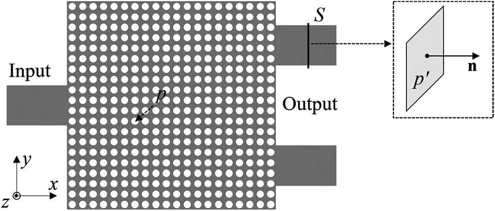
    Fig. 1. Schematic diagram of the single-mode 3 dB power divider (before optimization).
    3 dB power divider. The optimized (a) analog and (b) quasi-digital patterns in the first and second stages, respectively. (c) The optimized ternary pattern in which the smaller air cylinders with a radius of 35 nm are highlighted in orange. (d) Simulated excess loss profiles for the three patterns. (e) Measured excess loss profiles and (f) the SEM image of the fabricated device based on the ternary pattern. Inset in (e) shows the simulated steady-state intensity distribution.
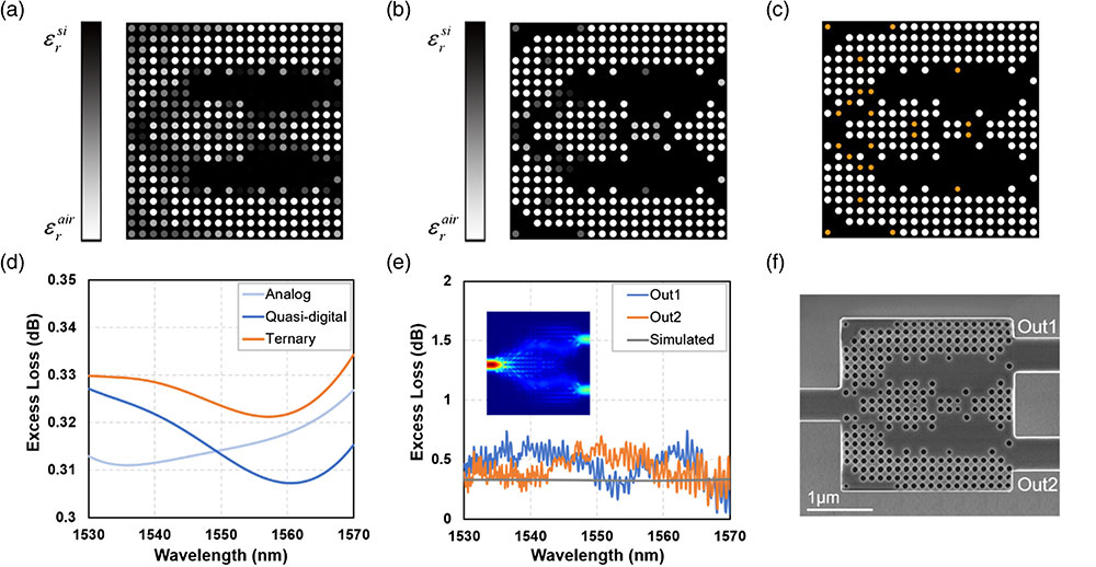
    Fig. 2. 3 dB power divider. The optimized (a) analog and (b) quasi-digital patterns in the first and second stages, respectively. (c) The optimized ternary pattern in which the smaller air cylinders with a radius of 35 nm are highlighted in orange. (d) Simulated excess loss profiles for the three patterns. (e) Measured excess loss profiles and (f) the SEM image of the fabricated device based on the ternary pattern. Inset in (e) shows the simulated steady-state intensity distribution.
    Schematic diagram of the dual-mode demultiplexer (before optimization).
    Fig. 3. Schematic diagram of the dual-mode demultiplexer (before optimization).
    Dual-mode demultiplexer. The optimized (a) analog and (b) quasi-digital patterns in the first and second stages, respectively. (c) The optimized ternary pattern in which the smaller air cylinders with a radius of 36 nm are highlighted in orange. (d) Simulated insertion loss and crosstalk profiles for the ternary pattern. Insets show the simulated steady-state intensity distributions of TE0 and TE1 modes, respectively. (e) and (f) Respectively, simulated and measured performance of a mode-division multiplexing system composed of a dual-mode multiplexer and a demultiplexer based on the ternary pattern. (g) and (h) Respectively, SEM images of the fabricated device based on the ternary pattern and the mode-division multiplexing system.
    Fig. 4. Dual-mode demultiplexer. The optimized (a) analog and (b) quasi-digital patterns in the first and second stages, respectively. (c) The optimized ternary pattern in which the smaller air cylinders with a radius of 36 nm are highlighted in orange. (d) Simulated insertion loss and crosstalk profiles for the ternary pattern. Insets show the simulated steady-state intensity distributions of TE0 and TE1 modes, respectively. (e) and (f) Respectively, simulated and measured performance of a mode-division multiplexing system composed of a dual-mode multiplexer and a demultiplexer based on the ternary pattern. (g) and (h) Respectively, SEM images of the fabricated device based on the ternary pattern and the mode-division multiplexing system.
    Kaiyuan Wang, Xinshu Ren, Weijie Chang, Longhui Lu, Deming Liu, Minming Zhang. Inverse design of digital nanophotonic devices using the adjoint method[J]. Photonics Research, 2020, 8(4): 528
    Download Citation