
Gang Qin, Fengqiang Ji, Likun Xia, Weiye Chen, Dongsheng Li, Jincheng Kong, Yanhui Li, Jianhua Guo, Shouzhang Yuan. HgCdTe high operation temperature infrared detectors[J]. Infrared and Laser Engineering, 2021, 50(4): 20200328
- Infrared and Laser Engineering
- Vol. 50, Issue 4, 20200328 (2021)
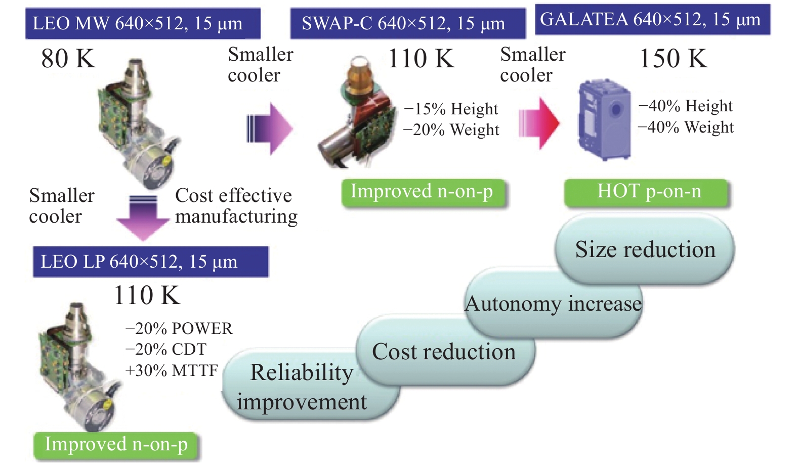
Fig. 1. Comparison of parameters of MW infrared detectors at different working temperatures
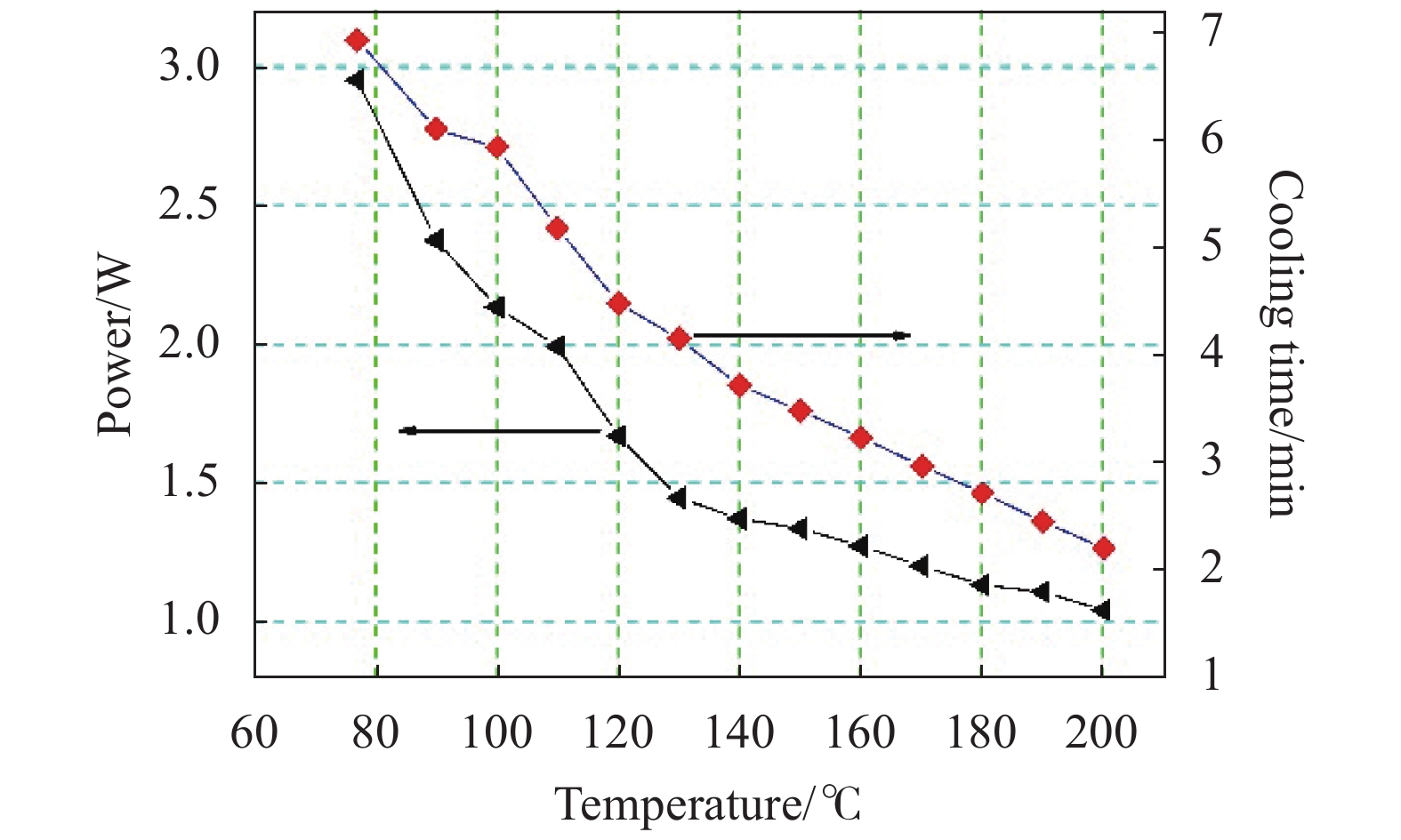
Fig. 2. Steady state power consumption and cooling time of cryocooler at different working temperature
Fig. 3. Imaging effect of p-on-n middle wavelength detector in AIM Co.
Fig. 4. Structure of P+/π(v )/N+ device
Fig. 5. Bandgap structure of HgCdTe nBn device
Fig. 6. Structure of device in unbalanced mode in DRS Co
Fig. 7. Distribution of As ion after injection and diffusion
Fig. 8. P+/v /N+ HgCdTe device structure of Teledyne
Fig. 9. Sample of barrier HgCdTe cell device in Military Technical University at Warsaw
Fig. 10. Relationship between the intrinsic carrier concentration and temperature at x =0.3
Fig. 11. Relationship between the intrinsic carrier concentration and temperature at x =0.22
Fig. 12. Relationship between dark current density and working temperature of detectors
Fig. 13. PSD of MWIR p-on-n devices at 140 K
Fig. 14. Number of RTS noise pixels detected as a function of the operating temperature for MWIR devices
Fig. 15. (a) SRH G-R current ; (b) Trap assisted tunneling current
Fig. 16. Relationship between Auger lifetime and temperature at x =0.3
Fig. 17. Relationship between Auger lifetime and temperature at x =0.22
Fig. 18. Relationship between Auger lifetime and temperature atx =0.3
Fig. 19. Carrier transport schematic of nBn devices under reverse bias
Fig. 20. Energy band configuration of HgCdTe heterojunctions
Fig. 21. Structure, energy band and carrier distribution of P+/v /N+ and P+/π/N+ devices
Fig. 22. Relationship between depletion width and reverse bias voltage with different absorption layer doping concentration

Set citation alerts for the article
Please enter your email address
© Copyright 2018-2021 | Chinese Laser Press. All Rights Reserved 沪ICP备15018463号-20