• Journal of Semiconductors
  • Vol. 43, Issue 12, 120401 (2022)
Xiaotian Sun1、*, Qiuhui Li3, Ruge Quhe2、**, Yangyang Wang4, and Jing Lu3、5、6、7、8、***
Author Affiliations
  • 1College of Chemistry and Chemical Engineering, and Henan Key Laboratory of Function-Oriented Porous Materials, Luoyang Normal University, Luoyang 471934, China
  • 2State Key Laboratory of Information Photonics and Optical Communications and School of Science, Beijing University of Posts and Telecommunications, Beijing 100876, China
  • 3State Key Laboratory for Mesoscopic Physics and School of Physics, Peking University, Beijing 100871, China
  • 4Qian Xuesen Laboratory of Space Technology, China Academy of Space Technology, Beijing 100094, China
  • 5Collaborative Innovation Center of Quantum Matter, Beijing 100871, China
  • 6Beijing Key Laboratory for Magnetoelectric Materials and Devices (BKL-MEMD), Peking University, Beijing 100871, China
  • 7Peking University Yangtze Delta Institute of Optoelectronics, Nantong 226010, China
  • 8Key Laboratory for the Physics and Chemistry of Nanodevices, Peking University, Beijing 100871, China
  • show less
    DOI: 10.1088/1674-4926/43/12/120401 Cite this Article
    Xiaotian Sun, Qiuhui Li, Ruge Quhe, Yangyang Wang, Jing Lu. Super high maximum on-state currents in 2D transistors[J]. Journal of Semiconductors, 2022, 43(12): 120401 Copy Citation Text show less
    References

    [1] Y Liu, X D Duan, H J Shin et al. Promises and prospects of two-dimensional transistors. Nature, 591, 43(2021).

    [2] M Y Li, S K Su, H S P Wong et al. How 2D semiconductors could extend Moore's law. Nature, 567, 169(2019).

    [3] Y Y Wang, S Q Liu, Q H Li et al. Schottky barrier heights in two-dimensional field-effect transistors: From theory to experiment. Rep Prog Phys, 84, 056501(2021).

    [4] R G Quhe, L Xu, S Q Liu et al. Sub-10 nm two-dimensional transistors: Theory and experiment. Phys Rep, 938, 1(2021).

    [5] P C Shen, C Su, Y X Lin et al. Ultralow contact resistance between semimetal and monolayer semiconductors. Nature, 593, 211(2021).

    [6] L Liu, T T Li, L Ma et al. Uniform nucleation and epitaxy of bilayer molybdenum disulfide on sapphire. Nature, 605, 69(2022).

    [7] Z Y Ni, M Ye, J H Ma et al. Performance upper limit of sub-10 nm monolayer MoS 2 transistors. Adv Electron Mater, 2, 1600191(2016).

    [8] R X Wu, Q Y Tao, J Li et al. Bilayer tungsten diselenide transistors with on-state currents exceeding 1.5 milliamperes per micrometre. Nat Electron, 5, 497(2022).

    [9] X T Sun, L Xu, Y Zhang et al. Performance limit of monolayer WSe 2 transistors; significantly outperform their MoS 2 counterpart. ACS Appl Mater Interfaces, 12, 20633(2020).

    [10] C G Qiu, Z Y Zhang, M M Xiao et al. Scaling carbon nanotube complementary transistors to 5-nm gate lengths. Science, 355, 271(2017).

    [11] The International Technology Roadmap for Semiconductors (ITRS). Online available,https://irds.ieee.org/editions/2021

    [12] The International Roadmap for Devices and Systems (IRDS). Online available:https://ieeexplore.ieee.org/abstract/document/7046976

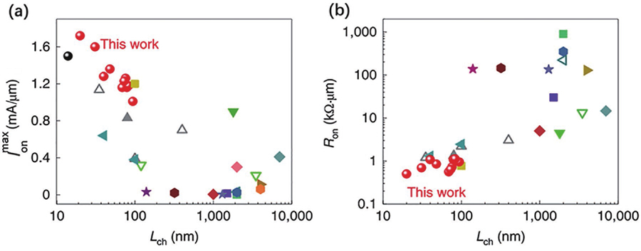
    [13] S Natarajan, M Agostinelli, S Akbar et al. A 14nm logic technology featuring 2nd-generation FinFET, air-gapped interconnects, self-aligned double patterning and a 0.0588 µm 2 SRAM cell size. 2014 IEEE International Electron Devices Meeting, 3.7.1(2014).

    [14] Y C Zhang, J Yu, R X Zhu et al. A single-crystalline native dielectric for two-dimensional semiconductors with an equivalent oxide thickness below 0.5 nm. Nat Electron, 5, 643(2022).

    Xiaotian Sun, Qiuhui Li, Ruge Quhe, Yangyang Wang, Jing Lu. Super high maximum on-state currents in 2D transistors[J]. Journal of Semiconductors, 2022, 43(12): 120401
    Download Citation