Author Affiliations
1College of Chemistry and Chemical Engineering, and Henan Key Laboratory of Function-Oriented Porous Materials, Luoyang Normal University, Luoyang 471934, China2State Key Laboratory of Information Photonics and Optical Communications and School of Science, Beijing University of Posts and Telecommunications, Beijing 100876, China3State Key Laboratory for Mesoscopic Physics and School of Physics, Peking University, Beijing 100871, China4Qian Xuesen Laboratory of Space Technology, China Academy of Space Technology, Beijing 100094, China5Collaborative Innovation Center of Quantum Matter, Beijing 100871, China6Beijing Key Laboratory for Magnetoelectric Materials and Devices (BKL-MEMD), Peking University, Beijing 100871, China7Peking University Yangtze Delta Institute of Optoelectronics, Nantong 226010, China8Key Laboratory for the Physics and Chemistry of Nanodevices, Peking University, Beijing 100871, Chinashow less
Very recently, a record
of 1720μA/μm among all the current 2D-material transistors (Fig. 1) accompanied by a small on-state resistance of 500 Ω·μm is achieved by Duan’s group from Hunan Univeristy in the 20 nm-channel-length BL WSe2 transistor with van der Waals (vdW) VSe2 contact[8].
is 1360μA/μm underVds = 0.8 V, which is also close to a prediction (~ 1500μA/μm) for the ML WSe2 MOSFET atVds = 0.72 V based on the ab initio quantum transport simulation by Luet al.[9]. Such a high performance can be ascribed to depression of the FLP in weak vdW contact[3].
Due to lack of reliable and sustainable doping technique, 2D semiconductors often need to contact metal electrods directly. Schottky barrier is often generated at the metal–semiconductor interface, resulting a poor contact. Schottky barrier originates from the the Fermi level pinng (FLP), which is caused by metal-induced gap states (MIGS)[3]. Because the Fermi level of semimetal Bi aligns with the conduction of the monolayer (ML) MoS2, the MIGS and thus FLP are greatly depressioned at the interface between Bi and ML MoS2[5]. With semimetal Bi as electrodes, Ohmic contact with ultra-low contact resistance of 123 Ω·µm and an
up to 1135μA/μm are obtained in a ML MoS2 transistor by Konget al. from MIT in 2021[5]. Compared with the ML MoS2, bilayer (BL) MoS2 has a narrower bandgap and higher electron density, which is beneficial for the on-state current enhancement. Recently, Wang’s group from Najing University has fabricated the BL MoS2 field-effect transistors with Bi as electrodes, and the mobility has improved by 37.9% and reached 122.6 cm2/(V·s), and
is further increased to 1270μA/μm[6]. The
values of these MoS2 transistors are consistent with that (~1200μA/μm) predicted based on the ab initio quantum transport simulation for the ML MoS2 transistor by Luet al. from Peking University[7].
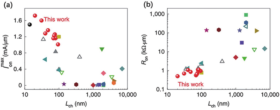
![(Color online) Benchmarking sub-100-nm bilayer WSe2 transistors (red ball) against the (a)Ionmaxfor 2D semiconductor transistors (b-P, b-As, b-AsP, MoS2, MoS2-0.7 nm, WSe2-0.7 nm, WS2, WS2-0.7 nm, MoTe2, GeAs, InSe, SnSe, ReS2, PtSe2, ZrSe2, HfSe2) andIon of 2021 silicon transistor (black ball) reported in ITRS, and (b) theRonmin(lowest on-state resistance) with those reported in the literature[8]. Reproduced with permission from Springer Nature, copyright 2022.](/Images/icon/loading.gif)
Figure 1.(Color online) Benchmarking sub-100-nm bilayer WSe2 transistors (red ball) against the (a)
for 2D semiconductor transistors (b-P, b-As, b-AsP, MoS2, MoS2-0.7 nm, WSe2-0.7 nm, WS2, WS2-0.7 nm, MoTe2, GeAs, InSe, SnSe, ReS2, PtSe2, ZrSe2, HfSe2) andIon of 2021 silicon transistor (black ball) reported in ITRS, and (b) the
(lowest on-state resistance) with those reported in the literature[8]. Reproduced with permission from Springer Nature, copyright 2022.
Although such
values in the 2D MoS2 and WSe2 transistors are comparable with or even exceedsIon in the Si transistors, it does not imply that the 2D transistors have outperformed the Si transistors as the carbon nanotube transistors do, reported by Penget al.[10]. The reason lies in the fact that the high
values of the best 2D WSe2 and MoS2 transistors are generated in a rather high gate swing (20–60 V)[6,8]. However, the Si FETs required in ITRS or IRDS operate under a small supply voltageVdd (about 0.7 V)[11,12], andIon is measured under a gate swing no more than thisVdd. To be specific,Ion is obtained under a biasVds and gate swing ofVg(on) –Vg(off) defined byVdd (Namely,Vds =Vg(on) –Vg(off) =Vdd). Given the same criterion, not onlyIon but also the closely related maximum transconductancegm of the best 2D WSe2 and MoS2 transistors remain much smaller than those of the Si transistors under the similarVdd [0.15–5 (MoS2 and WSe2) vs 1000μA/μm (Si) inIon and 0.13–20 (MoS2 and WSe2) vs 3000μS/μm (Si) in gm][6,8,13].
Two-dimensional (2D) materials have been recognized as a type of potential channel material to replace silicon in future field-effect transistors (FETs) by the International Technology Roadmap for Semiconductors (ITRS) and its succesor the International Roadmap for Devices and Systems (IRDS)[1-4]. Substantial first principle quantum transport simulations have predicted that many 2D transistors, including those with MoS2, WSe2, phosphorene, and Bi2O2Se channels, own excellent device performance and are able to extend Moore’s law down to the sub-10 nm scale[4]. However, the actual 2D transistors suffer from poor contact and dielectric[4]. As a result, the maximum on-state currents (
) or saturation currents (Isat) of the fabricated 2D transistors are even generally lower than the on-state current (Ion) (>1200μA/μm) of the most advanced silicon transistors. As we know, the on-state current is one of the most critical figure of merit of a FET required by ITRS and IRDS, and a large on-state current implies a fast switching speed.
The improvement method is to use the high-κ dielectric with ultrathin thickness and obtain an ultrasmall equivalent oxide thickness (EOT)[1]. Duanet al. have tried to reduce the EOT of the bilayer WSe2 FETs by using the 3-nm Al2O3/6-nm HfO2 dielectric layer. The corresponding gate swing is significantly decreased from 40 to below 5 V,
remains over 1 mA/μm[8], andgm is significantly improved from 0.13 to 150μS/μm. Very recently, Penget al. from Peking University have successfully fabricated the sub-0.5-nm EOT (2.3-nmβ-Bi2SeO5) in the 2D Bi2O2Se FETs, realizing ultralow leakage current[14]. This achievement overcomes the challenges in depositing the ultra-thin gate dielectric on the dangling-bond-free 2D semiconductors, making it promising for the development of 2D transistors with highIon andgm.
References
[1] Y Liu, X D Duan, H J Shin et al. Promises and prospects of two-dimensional transistors. Nature, 591, 43(2021).
[2] M Y Li, S K Su, H S P Wong et al. How 2D semiconductors could extend Moore's law. Nature, 567, 169(2019).
[3] Y Y Wang, S Q Liu, Q H Li et al. Schottky barrier heights in two-dimensional field-effect transistors: From theory to experiment. Rep Prog Phys, 84, 056501(2021).
[4] R G Quhe, L Xu, S Q Liu et al. Sub-10 nm two-dimensional transistors: Theory and experiment. Phys Rep, 938, 1(2021).
[5] P C Shen, C Su, Y X Lin et al. Ultralow contact resistance between semimetal and monolayer semiconductors. Nature, 593, 211(2021).
[6] L Liu, T T Li, L Ma et al. Uniform nucleation and epitaxy of bilayer molybdenum disulfide on sapphire. Nature, 605, 69(2022).
[7] Z Y Ni, M Ye, J H Ma et al. Performance upper limit of sub-10 nm monolayer MoS 2 transistors. Adv Electron Mater, 2, 1600191(2016).
[8] R X Wu, Q Y Tao, J Li et al. Bilayer tungsten diselenide transistors with on-state currents exceeding 1.5 milliamperes per micrometre. Nat Electron, 5, 497(2022).
[9] X T Sun, L Xu, Y Zhang et al. Performance limit of monolayer WSe 2 transistors; significantly outperform their MoS 2 counterpart. ACS Appl Mater Interfaces, 12, 20633(2020).
[10] C G Qiu, Z Y Zhang, M M Xiao et al. Scaling carbon nanotube complementary transistors to 5-nm gate lengths. Science, 355, 271(2017).
[11] The International Technology Roadmap for Semiconductors (ITRS). Online available,https://irds.ieee.org/editions/2021
[12] The International Roadmap for Devices and Systems (IRDS). Online available:https://ieeexplore.ieee.org/abstract/document/7046976
[13] S Natarajan, M Agostinelli, S Akbar et al. A 14nm logic technology featuring 2nd-generation FinFET, air-gapped interconnects, self-aligned double patterning and a 0.0588 µm 2 SRAM cell size. 2014 IEEE International Electron Devices Meeting, 3.7.1(2014).
[14] Y C Zhang, J Yu, R X Zhu et al. A single-crystalline native dielectric for two-dimensional semiconductors with an equivalent oxide thickness below 0.5 nm. Nat Electron, 5, 643(2022).