
Side Song, Guozhu Liu, Hailiang Zhang, Lichao Chao, Jinghe Wei, Wei Zhao, Genshen Hong, Qi He. Reliability evaluation on sense-switch p-channel flash[J]. Journal of Semiconductors, 2021, 42(8): 084101
- Journal of Semiconductors
- Vol. 42, Issue 8, 084101 (2021)
Abstract
1. Introduction
With the rapid development of aerospace technology, the demand for highly qualified and highly reliable electrical and electronic systems is stronger and stronger. FPGA (field programmable gate array) is an important class of integrated circuit device used in aerospace electronics. There are mainly three kinds of FPGAs, the antifuse-based FPGA[
To the best of our knowledge, the configuration cells for flash-based FPGA mainly include sense-switch and push-pull[
In this letter, the reliability of sense-switch p-channel flash was evaluated with emphasis on endurance and data retention. It is assured that the sense-switch p-channel flash could be programmed and erased for more than 10 000 cycles with only 1.3 V threshold voltage window closing and 30% drive current degradation. The data retention ability at 150 °C is extrapolated to be 5 years (when a criteria of 30% degradation in drive current is used); moreover, the electrical parameters of the p-channel flash at different temperature are monitored. All the results indicate that the sense-switch p-channel flash has the potential to be applied into flash-based FPGA.
2. Experiment
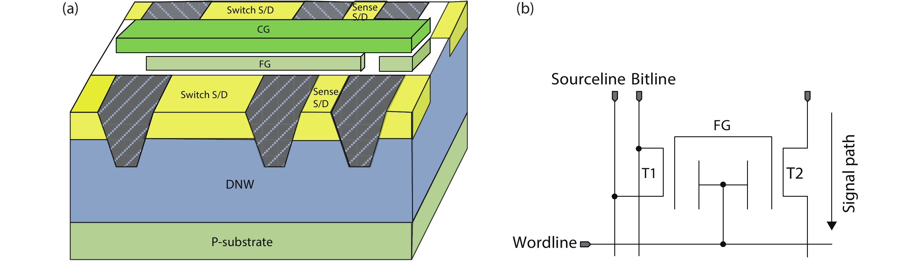
The sense-switch p-channel flash was manufactured using 130 nm embedded flash technology. Fig. 1(a) depicts the cell structure. A sense-switch device consists of two transistors, the sense transistor, which is used for program, erase and verify operations, and the switch, which is randomly wired to logic devices for signal propagation. It is noted that both the sense (T1) and switch (T2) transistor share the same control gate and floating gate, when T1 is programmed, the floating gate will be filled with electron and the channel of T2 is turned on. When T1 is erased, the electron is ejected from the common floating gate and T2 is turned off, as shown in Fig. 1(b).
![]()
Figure 1.(Color online) (a) The three-dimensional sense-switch p-channel flash diagram. (b) The basic working schematic.
The reliability evaluation is mainly focused on endurance and data retention. For endurance evaluation, the devices are programmed and erased for as long as 10 000 cycles, the electric characteristics were monitored. The data retention ability is tested at both the room temperature and high temperature for a typical stress duration. Last but not least, the I–V characteristics of the sense-switch p-channel flash at different temperature are measured. For each evaluation, at least five devices are chosen to increase the accuracy. It should be noted that all the device characteristics monitored in the following were limited only to the switch transistor (T2).
3. Results and discussion
3.1. Endurance
The threshold voltage (Vth, collected by constant current at Id = –0.1 μA) and drive current (Ion = Id @ Vd = –1.5 V, Vcg = 0 V) as a function of program and erase cycles is shown in Fig. 2(a). Both the Vth after programming and erasing shift toward the negative direction, where the programmed Vth sees a larger shift (2.5 V) than the erased Vth (1.2 V), resulting in a Vth window closing from 11.1 V at initial to 9.7 V from the initial to 10 000 program and erase cycles. The drive current exhibits a first slow and then fast drop-down phenomenon, and the drive current decreases about 30% up to 10 000 cycles.
![]()
Figure 2.(Color online) (a) The threshold voltage and drive current as a function of the program and erase cycles. (b) Electron trapping in the tunnel oxide or spacer at the drain side when programmed.
The reasons for Vth shift and drive current degradation are in close link with the tunnel oxide and spacer at the drain side[
where ΔQ is the density of trapped electrons in the tunnel oxide, ε is the dielectric constant of the tunnel oxide and d is the thickness of the tunnel oxide. Lower programmed Vth means less electron on the common floating gate, which in turn increases the channel resistance of the switch transistor, leading to an obvious drop-down of the drive current.
After all, the sense-switch p-channel flash is endurable to more than 10 000 program and erase cycles, in comparison to the sense-switch n-channel flash (more than 1000 program and erase cycles[
3.2. Data retention
The evaluation on sense-switch p-channel flash’s data retention ability is carried out both in room temperature and high temperature. Fig. 3(a) is the current-time curve measured with drain bias at –1.5 V, control gate bias at 0 V, grounded source and substrate for the programmed state switch transistor at room temperature. Fig. 3(b) depicts the I–V characteristic of the sense-switch p-channel flash before and after 100 000 s read stress. Both curves show that the p-channel flash is unaffected by room temperature read stress.
![]()
Figure 3.(Color online) (a) Current–time curve during read stress at room temperature. (b)
The high temperature data retention experiment is carried out both for the programmed and erased flash devices, with a typical bake temperature (150 °C) and time (1000 h), the results are shown in Figs. 3(c)–3(f). Figs. 3(c) and 3(d) represent the p-channel flash without and with 500 program and erase cycles before the bake process, respectively. For those without being cycled before baking, the Vth shift is about 1 V, in comparison to 0.4 V for the device with 500 program and erase cycles, in the first 150 °C, 168 h bake duration. While in the next 168–1000 h duration, both devices exhibit a similar Vth shift of about 0.5 V. Two possible reasons are proposed to explain the difference: Firstly, those devices without cycling first before baking have a more positive threshold voltage (~6.8 V), corresponding to larger amount of electrons on the floating gate and lower intrinsic potential, when they are subjected to high temperature bake, more electron can gain energy and escape either through the tunnel oxide[
Fig. 3(e) reports the degradation of drive current (collected at Vd = –1.5 V and Vcg = Vb = Vs = 0 V) as function of the high temperature bake time, the data fit a log-linear relationship that can be extrapolated to 30% degradation at 43 000 h (about 5 years) and 40% degradation at 470 000 h (about 53 years), at 150 °C, in comparison to Microsemi’s RT ProASIC3 devices’ data retention (less than 10 years at 150 °C). Moreover, the erased state p-channel flash under high temperature bake was also investigated, as shown in Fig. 3(f), and no obvious change was found in the 150 °C, 1000 h time duration. The results above indicate that the sense-switch p-channel flash has good data retention properties under high temperature ambient.
3.3. Temperature related performance
The electrical parameters of the sense-switch p-channel flash under different temperature conditions are also tested, as reported in Fig. 4. The drive current of programmed state at Vd = –1.5 V and Vcg = 0 V (see Fig. 4(a)) increases about 10% (at –55 °C) and drops about 14% (at 125 °C) in comparison with the value measured at room temperature (25 °C). The Vth shift (see Fig. 4(b)) is less than 1 V in the –55 to 125 °C temperature range. Specifically, a thermal cycling experiment between 25 and 125 °C is carried out and the result is reported in Fig. 4(c). Except for the first two cycles, where the Vth and drive current drops a little, the next cycles are quite stable and reproducible. The results above show that the sense-switch p-channel flash is robust in low and high temperature, even with a sudden change of the temperature, once again lays a foundation for the investigation of sense-switch p-channel flash used as configuration cells for flash-based FPGA.
![]()
Figure 4.(Color online) (a) The output characteristics of the programmed switch. (b) The programmed and erased state of the switch under different temperatures. (c) The threshold voltage and drive current with different temperature cycling.
4. Conclusion
The reliability of sense-switch p-channel flash concerning endurance and data retention were evaluated on emphasis. The endurance experiment suggests that the sense-switch p-channel flash could be programmed and erased for more than 10 000 cycles with only 1.3 V threshold voltage window closing and 30% drive current degradation, which is mainly due to the electron trapping in the tunnel oxide or spacer at the drain side. The room temperature read stress has a negligible effect on the p-channel flash, and the data retention ability at 150 °C is extrapolated to be 5 years (when a criteria of 30% degradation in drive current is used) and about 53 years (when a criteria of 40% degradation in drive current is used). Furthermore, the p-channel flash is proved to be robust and endurable at different temperatures or suffer from a sudden temperature change. All the results indicate that the sense-switch p-channel flash is a potential configuration cell for flash-based FPGA.
References
[1] G Z Liu. Characterization and modeling of a highly reliable ONO antifuse for high-performance FPGA and PROM. Int J Mater Sci Appl, 5, 169(2016).
[2] T N He, F C Zhang, S Bhunia et al. Silicon carbide (SiC) nanoelectromechanical antifuse for ultralow-power one-time-programmable (OTP) FPGA interconnects. IEEE J Electron Devices Soc, 3, 323(2015).
[3] N Rezzak, D Dsilva, J J Wang et al. SET and SEFI characterization of the 65 nm SmartFusion2 flash-based FPGA under heavy ion irradiation. 2015 IEEE Radiation Effects Data Workshop, 1(2015).
[4] J Zhang, D M Zhou. An 8.5-ps two-stage vernier delay-line loop shrinking time-to-digital converter in 130-nm flash FPGA. IEEE Trans Instrum Meas, 67, 406(2018).
[5] X L Li, Q K Yu, Y Sun et al. The experimental study on SEU hardened effect of flash FPGA for space application. 2018 International Conference on Radiation Effects of Electronic Devices, 1(2018).
[6] S Rezgui, J J Wang, E C Tung et al. New methodologies for SET characterization and mitigation in flash-based FPGAs. IEEE Trans Nucl Sci, 54, 2512(2007).
[7] M Ebrahimi, P M B Rao, R Seyyedi et al. Low-cost multiple bit upset correction in SRAM-based FPGA configuration frames. IEEE Trans Very Large Scale Integr (VLSI) Syst, 24, 932(2016).
[8] C Bernardeschi, L Cassano, A Domenici. SRAM-based FPGA systems for safety-critical applications: A survey on design standards and proposed methodologies. J Comput Sci Technol, 30, 373(2015).
[9] J J Wang, N Rezzak, D Dsilva et al. A novel 65 nm radiation tolerant flash configuration cell used in RTG4 field programmable gate array. IEEE Trans Nucl Sci, 62, 3072(2015).
[10] N Rezzak, J J Wang, D Dsilva et al. TID and SEE characterization of microsemi's 4th generation radiation tolerant RTG4 flash-based FPGA. 2015 IEEE Radiation Effects Data Workshop, 1(2015).
[11]
[12] G Z Liu, B Li, J H Wei et al. A radiation-hardened Sense-Switch pFLASH cell for FPGA. Microelectron Reliab, 103, 113514(2019).
[13] G Z Liu, B Li, Z Q Xiao et al. The TID characteristics of a radiation hardened sense-switch pFLASH cell. IEEE Trans Device Mater Reliab, 20, 358(2020).
[14] S Yamada, Y Hiura, T Yamane et al. Degradation mechanism of flash EEPROM programming after program/erase cycles. Proc IEEE Int Electron Devices Meet, 23(1993).
[15] B A Schmid, J Y Jia, J Wolfman et al. Cycling induced degradation of a 65 nm FPGA flash memory switch. IEEE International Integrated Reliability Workshop Final Report, 92(2010).
[16] S S Chung, S N Kuo, C M Yih et al. Performance and reliability evaluations of p-channel flash memories with different programming schemes. Int Electron Devices Meet IEDM Tech Dig, 295(1997).
[17] R E Shiner, J M Caywood, B L Euzent. Data retention in EPROMS. 18th International Reliability Physics Symposium, 238(1980).
[18] S Mori, Y Kaneko, N Arai et al. Reliability study of thin inter-poly dielectrics for non-volatile memory application. 28th Annual Proceedings on Reliability Physics Symposium, 132(1990).

Set citation alerts for the article
Please enter your email address
© Copyright 2018-2021 | Chinese Laser Press. All Rights Reserved 沪ICP备15018463号-20