
Xuyang Wang, He Jia, Junhui Li, Yumei Guo, Yu Liu. Optical transmitter module with hybrid integration of DFB laser diode and proton-exchanged LiNbO3 modulator chip[J]. Journal of Semiconductors, 2022, 43(6): 062303
- Journal of Semiconductors
- Vol. 43, Issue 6, 062303 (2022)
Abstract
1. Introduction
Lithium niobate (LiNbO3) single crystals have been recognized as the most mature material for electro-optic modulators thanks to their Pockels effect[
In recent years, radio-frequency (RF) photonics technology (e.g., microwave photonics radars and electronic warfare systems) has rapidly matured, and continues to develop toward miniaturization and integration[
The DFB laser chip and the LiNbO3 modulator chip are made of different materials. Several methods can be used to integrate laser chips and modulator chips, such as via lenses[
2. Schematic design
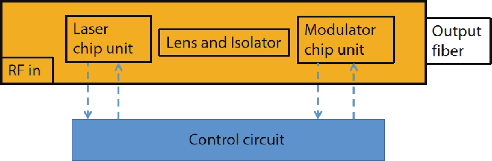
The layout of the transmitter module is illustrated in Fig. 1. The module comprises a laser chip unit, a lens, an optical isolator, a broadband LiNbO3 Mach–Zehnder modulator chip unit, and fibers. The housing material is Kovar. The size of the whole package is minimized by design.
![]()
Figure 1.(Color online) Diagrammatic sketch of the module.
The laser unit includes a distributed feedback (DFB) laser chip, a monitor photodetector (PD), a thermistor, and a control circuit. The laser chip unit is installed with a heat sink and TEC (Thermo Electric Cooler). The DFB laser works with stable wavelength and stable power under the control of the current and the TEC through the real-time feedback of the monitor PD and the thermistor[
![]()
Figure 2.(Color online) Diagrammatic sketch of the laser chip unit.
The light emitted by the DFB laser chip is coupled to the input optical waveguide of the modulator chip through a spatial lens, an optical isolator, and a fiber-tail. The modulator chip unit comprises a microstrip, a LiNbO3 modulator chip, a photodetector, and a bias control circuit, as shown in Fig. 3.
![]()
Figure 3.(Color online) Sketch of the modulator chip unit.
The radio frequency (RF) signal is loaded to the modulator chip through a microwave connector and a microstrip on the shell, connecting the RF connector and the modulator chip electrode. A traveling-wave electrode structure is adopted on the modulator chip[
The LiNbO3 Mach–Zehnder modulator must work at the quadrature point[
The output light beam of the modulator chip is coupled into an optical fiber that is attached to the output end of the modulator chip and it then goes out from the whole module.
3. Simulation
The simulation consists of two parts: the optical path design and the modulator chip design. The positions and parameters of each optical unit (e.g., the lens, isolator, and fiber) were optimized to maximize the optical output efficiency of the whole module. The modulator chip's waveguide and traveling-wave electrode structure were also designed to obtain a high on-off extinction ratio, a wide bandwidth, and a low insertion loss.
Fig. 4 shows the optical coupling path of the module. The output beam from the laser chip goes through a subassembly comprising a microlens and a microisolator, which rotates the polarization direction of the light by 45°.
![]()
Figure 4.(Color online) Optical path of the module.
There are several mature LiNbO3 waveguide fabrication methods, such as the ridge waveguide method[
![]()
Figure 5.(Color online) Simulation results of normalized optical output efficiency of the module vs. (a) rotated angle of the fiber, (b) optical axis offset distance of the lens, (c) optical axis offset distance of the fiber to the cocenter optical axis, and (d) the MFD of the modulator waveguide.
The parameters and positions of the laser chip, the lens, and the fiber (e.g., the numerical aperture and focal length of the lens) are calculated and optimized to achieve the maximum optical output efficiency. The optical axis of each component must be strictly located in a straight line to avoid the optical loss caused by the offset of each unit. Figs. 5(b) and 5(c) shows the optical output efficiency's dependence on the optical axis offset of the lens and the fiber to the cocenter optical axis of the whole module.
What can be observed and inferred from Figs. 5(b) and 5(c) is that the optical output efficiency is much more sensitive to the optical axis offset of the lens than the fiber. Therefore, the micro-assembly technology of the lens would be the critical point of module fabrication.
The optical output efficiency is also influenced by the mode field diameter (MFD) of the modulator waveguide, as shown in Fig. 5(d). The MFD of the communication fiber is approximately 10 μm, and the optical output efficiency reaches the maximum point when the MFD of the modulator waveguide is the same as that of the fiber. The mismatch of the MFD between the modulator waveguide and the fiber introduces extra coupling loss between the modulator chip and the fiber.
To obtain a high output extinction ratio of the module, the waveguide structure of the modulator should be well designed. The extinction ratio of the LiNbO3 modulator mainly depends on the optical intensity balance and coupling ratio between the two modulation arms. Fig. 6(a) is a schematic drawing of the MZ waveguide structure of the modulator. The incoming light signal splits into two arms through a Y-splitter. The optical intensity in Arm 1 is I1, and that in Arm 2 is I2. The angles between the input light signal and each Y-branch are θ1 and θ2, respectively. The optical phase in each arm can be modulated by an applied voltage. The in-phase traveling through the two arms will result in a maximum intensity output, while the out-phase traveling will result in a minimum intensity output after the combiner[
![]()
Figure 6.(Color online) (a) MZ-modulator waveguide structure. (b) Simulation results of extinction ratio (on/off) and split ratio variation vs. normalization angle. (c) Simulation results of extinction ratio (on/off) and coupling ratio vs. two arms distance.
Fig. 6(b) shows the relationship between the extinction ratio and the split ratio variation. The split ratio variation is defined as |(I1− I2)/(I1+ I2)|, and the normalization angle is defined as |θ1− θ2|. When θ1 equals θ2, the input optical intensity splits evenly into Arm 1 and Arm 2. The modulator's on/off extinction ratio reaches maximum. Fig. 6(c) shows the relationship between the extinction ratio and the optical power coupling ratio of the two modulator arms. When the optical powers of the two modulation arms couple, the extinction ratio decreases.
The module's bandwidth depends on the bandwidth of the modulator chip and the RF transmission loss of the microstrip line. The design of the traveling-wave electrode and the microstrip line should be optimized to satisfy the required bandwidth. Fig. 7 shows the simulated result of the electro-optic response of the module. The bandwidth of the module could reach up to 28 GHz.
![]()
Figure 7.Simulation results of the electro-optic response of the module.
4. Results and discussion
According to the assembly requirements of each unit, the sequence to construct the module was optimized as follows. First, the laser chip, monitor PD, and thermistor were mounted on the same heat sink and TEC. Then, the laser module was assembled into the designed shell. The laser chip control circuit was also connected. The modulator chip was coupled with the input and output fiber. It was then installed in the shell, connected with the modulator bias-control circuit. The hybrid integrated optical transmitter module is shown in Fig. 8. Online monitoring of the output optical power of the whole module was allowed. The maximum output optical power of the module was realized by constantly adjusting the position of the lens and isolator.
![]()
Figure 8.(Color online) Hybrid integrated optical transmitter module.
The DFB laser chip was able to provide over 70 mW of optical power with fewer than 1 MHz linewidths. Fig. 9 shows the tested characteristic curve of the laser chip.
![]()
Figure 9.
The waveguide of the modulator chip was fabricated using the proton exchange and annealing method. By adjusting the temperature and time of the process, the MFD of the waveguide approached the designed value. The overall insertion loss of the chip was 3.6 dB with both the input and output ends coupled with the polarization-maintaining single-mode fibers (PMSMF).
By continuously optimizing the chip structure and the fabrication process (e.g., the Y-branch structures of the waveguide, the photolithography process, and the electroplating process), the electro-optic (EO) bandwidth of the modulator chip reached 26.5 GHz (from 2 GHz) at 3 dB and the extinction ratio (ER) of the chip was better than 35 dB. The test results are shown in Fig. 10.
![]()
Figure 10.(a) EO bandwidth and (b) ER test results of the LiNbO3 modulator chip.
The optical output efficiency of the module obtained by simulation was 42.3%. However, the measured optical output efficiency was approximately 21%, as shown in Table 1. The reason for this may be that the parameters used in the simulation, such as the divergence angle of the laser and numerical aperture of the lens, were slightly different from the actual parameters. The inevitable offset of each unit and inaccurate tilted angle of the fiber during fabrication would also lead to a large deviation in the overall results.
The output optical power of the module depends on the optical power provided by the laser chip, the coupling loss from the laser chip to the fiber-tail, and the insertion loss of the modulator chip. In this work, the laser chip with 600 μm cavity length provides power over 70 mW, the coupling loss is about 3.2 dB, while the insertion loss is 3.6 dB. In future work, the following methods could be helpful to increase the output power of the module: applying higher power laser chips with longer cavity length, increasing the coupling efficiency by selecting the lens parameters in accordance with the actual divergence angle of the laser chip, or decreasing the insertion loss by optimizing the modulator chip's waveguide fabrication process to make the waveguide's mode field diameter match better with that of the optical fiber.
The measured bandwidth was 20.5 GHz (from 2 GHz), which is 6 GHz smaller than the modulator chip bandwidth caused by the microwave transmission loss along the microstrip. Fig. 11(a) shows the tested result. The difference between the simulation and the tested result was mainly caused by the deviations and defects of the modulator electrode structures and microstrip line during fabrication. The extinction ratio of the module was 34 dB, which is slightly smaller than that of the modulator chip. This might be due to the different measurement setups.
![]()
Figure 11.(a) EO bandwidth and (b) ER test results of the module.
The transmitter module's link p erformance parameters were also tested by connecting the transmitter module to a microwave system. When the input RF signal was 9 GHz, the noise figure (NF) of the system was 38.81 dB. The 1 dB compression point (P1 dB) was 19.5 dBm. The 3rd-order intercept point (IIP3) was 33.08 dBm, as shown in Fig. 12. The 3rd-order spur free dynamic range (SFDR3), which characterizes the linearity behavior of the module, can be shown to be equal to
![]()
Figure 12.(Color online) Output RF power of a linear tone and of a third-order intermodulation vs. the RF input power.
These performance metrics are consistent with those of a discrete system with identical test conditions.
SFDR3 is an essential parameter for analog modulation links. It can be improved by using a higher power and lower relative intensity noise laser chip, increasing the Vπ of the modulator chip appropriately, raising the optical coupling efficiency, and so on. However, increasing the modulator's Vπ will reduce the link's gain. Therefore, comprehensive consideration including the gain, noise figure, and SFDR3 should be taken according to the requirements of the system's applications.
5. Conclusion
By packaging the DFB laser chip and the LiNbO3 Mach–Zehnder modulator chip in one shell, a hybrid integrated optical transmitter module was realized with a significant reduction in volume compared to existing systems based on discretely packaged components. Moreover, by adopting the proton-exchange LiNbO3 waveguide fabrication scheme and optimizing the LiNbO3 waveguide structure and fabrication process, the extinction ratio of the module reaches 34 dB, while the typical extinction ratio of a discrete system is approximately 20 dB. The optical output efficiency of the hybrid integrated optical transmitter module reached approximately 21% with a 3 dB bandwidth of 20.5 GHz (from 2 GHz). The link performance parameters of the hybrid integrate module are comparable to those of a discrete system with identical test conditions. In the next stage, we will focus on the environmental adaptability of the transmitter module and its characteristics in the system.
Acknowledgements
This work was supported by National Key Research and Development Program of China (2018YFB2201101), the Strategic Priority Research Program of Chinese Academy of Sciences,Grant No. XDB43000000 and Beijing Municipal Science & Technology Commission,Administrative Commission of Zhongguancun Science Park No. Z201100004020004
References
[1] G L Li, P K L Yu. Optical intensity modulators for digital and analog applications. J Lightwave Technol, 21, 2010(2003).
[2] N Dagli. Wide-bandwidth lasers and modulators for RF photonics. IEEE Trans Microw Theory Tech, 47, 1151(1999).
[3] J N Huang, C Li, R G Lu et al. Beyond the 100 Gbaud directly modulated laser for short reach applications. J Semicond, 42, 041306(2021).
[4] D P Liu, J Tang, Y Meng et al. Ultra-low Vpp and high-modulation-depth InP-based electro–optic microring modulator. J Semicond, 42, 082301(2021).
[5] X X Wang, P O Weigel, J Zhao et al. Achieving beyond-100-GHz large-signal modulation bandwidth in hybrid silicon photonics Mach Zehnder modulators using thin film lithium niobate. APL Photonics, 4, 096101(2019).
[6] E L Wooten, K M Kissa, A Yi-Yan et al. A review of lithium niobate modulators for fiber-optic communications systems. IEEE J Sel Top Quantum Electron, 6, 69(2000).
[7] D Marpaung, C Roeloffzen, R Heideman et al. Integrated microwave photonics. Laser Photonics Rev, 7, 506(2013).
[8] Z Y Lu, Lu B, Y Luo et al. Design and research on small hybrid integrated teansmitter module of semiconductor and DFB laser. J Opto Laser, 32, 181(2021).
[9] Y Li, T Lan, J Li et al. High-efficiency edge-coupling based on lithium niobate on an insulator wire waveguide. Appl Opt, 59, 6694(2020).
[10] L Y Li, Y X Ma, Y S Zhang et al. Multi-tip edge coupler for integration of a distributed feedback semiconductor laser with a thin-film lithium niobate modulator. Appl Opt, 60, 4814(2021).
[11] M Qiu. Vertically coupled photonic crystal optical filters. Opt Lett, 30, 1476(2005).
[12] S Chakravarty, M Teng, R Safian et al. Hybrid material integration in silicon photonic integrated circuits. J Semicond, 42, 041303(2021).
[13] K Matsumoto, Y Kanaya, J Kishikawa et al. Characteristics of film InP layer and Si substrate bonded interface bonded by wafer direct bonding. 2015 11th Conference on Lasers and Electro-Optics Pacific Rim, 7375926(2015).
[14] M A Olmstead, F S Ohuchi. Group III selenides: Controlling dimensionality, structure, and properties through defects and heteroepitaxial growth. J Vac Sci Technol A, 39, 020801(2021).
[15]
[16] J Zhang, C X Gao, M Y Xue et al. Research on frequency modulation character of the current driven DFB semiconductor laser. Mod Phys Lett B, 33, 1850422(2019).
[17] R C Alferness. Waveguide electrooptic modulators. IEEE Trans Microwave Theory Tech, 30, 1121(1982).
[18]
[19]
[20] L L Wang, T Kowalcyzk. A versatile bias control technique for any-point locking in lithium niobate Mach–Zehnder modulators. J Lightwave Technol, 28, 1703(2010).
[21] G Yang, A V Sergienko, A Ndao. Tunable polarization mode conversion using thin-film lithium niobate ridge waveguide. Opt Express, 29, 18565(2021).
[22] M Fukuma, J Noda. Optical properties of titanium-diffused LiNbO3 strip waveguides and their coupling-to-a-fiber characteristics. Appl Opt, 19, 591(1980).
[23] G R Paz-Pujalt, D D Tuschel, G Braunstein et al. Characterization of proton exchange lithium niobate waveguides. J Appl Phys, 76, 3981(1994).
[24] A Méndez, la Paliza G de, A García-Cabañes et al. Comparison of the electro-optic coefficient r33 in well-defined phases of proton exchanged LiNbO3 waveguides. Appl Phys B, 73, 485(2001).


Set citation alerts for the article
Please enter your email address

© Copyright 2018-2021 | Chinese Laser Press. All Rights Reserved 沪ICP备15018463号-20