
Xiaochi Chen, Colleen S. Fenrich, Muyu Xue, Ming-Yen Kao, Kai Zang, Ching-Ying Lu, Edward T. Fei, Yusi Chen, Yijie Huo, Theodore I. Kamins, James S. Harris. Tensile-strained Ge/SiGe multiple quantum well microdisks[J]. Photonics Research, 2017, 5(6): B7
- Photonics Research
- Vol. 5, Issue 6, B7 (2017)
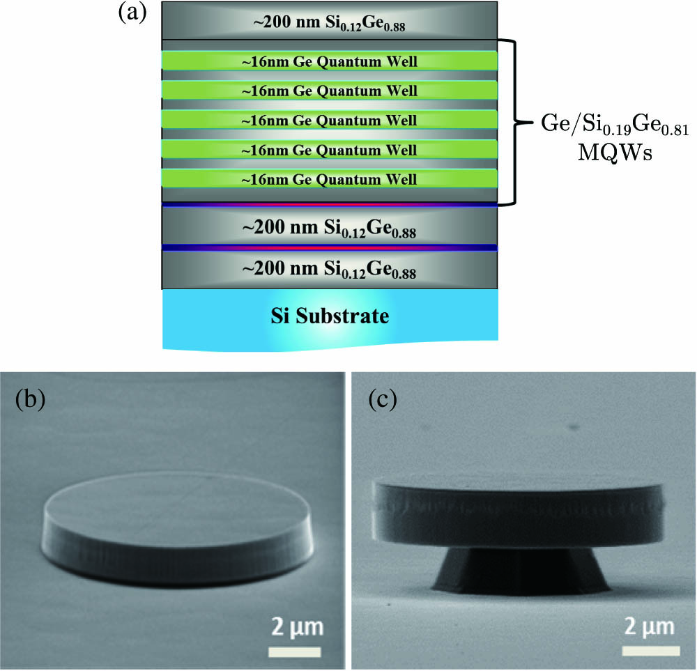
Fig. 1. Epitaxial stack design and the fabricated Ge/SiGe MQW microdisks. (a) Schematic of the Ge/SiGe MQW epitaxial structure. (b) Scanning electron microscope (SEM) image of a nonsuspended Ge/SiGe MQW microdisk. (c) SEM image of a suspended Ge/SiGe MQW microdisk supported by a Si post.
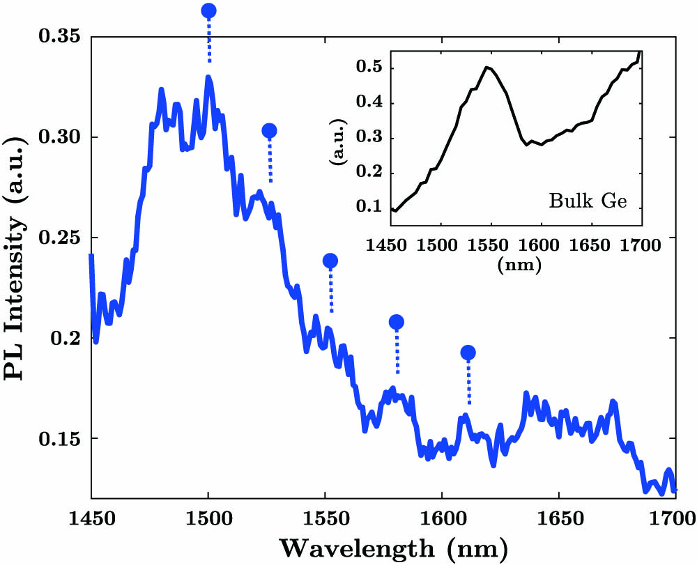
Fig. 2. Room-temperature PL of a suspended Ge/SiGe MQW microdisk exhibiting FP mode resonances. Inset: Bulk Ge reference showing direct bandgap emission at 1550 nm.
Fig. 3. 3D-FEM simulation for tensile-strained microdisks. (a) Schematic of type 1, type 2, and type 3 SiN x
Fig. 4. (a) Schematic of the epitaxial stack of the Ge/SiGe MQW microdisk. (b) Fabrication process flow for a tensile-strained, suspended Ge/SiGe MQW microdisk. (c) SEM image of a Ge/SiGe MQW microdisk without SiN x SiN x
Fig. 5. PL and Raman characterizations of Ge/SiGe MQW microdisks. (a) Room-temperature PL of strained (red and blue) and unstrained (black) microdisks. (b) Typical Raman spectrum from the center of a microdisk. (c) Raman line scan along the diameter of a strained, suspended Ge/SiGe MQW microdisk.
Fig. 6. Comparisons of simulation, PL, and Raman measurements. (a) Devices 1, 2 (440 nm thick, 6 μm diameter). (b) Devices 3, 4 (440 nm thick, 10 μm diameter). (c) Devices 5, 6 (340 nm thick, 6 μm diameter). (d) Devices 7, 8 (340 nm thick, 10 μm diameter).
Fig. 7. Optical gain calculations for Ge/SiGe MQW. (a) Band alignment of strain-balanced Ge / Si 0.19 Ge 0.81 Ge / Si 0.19 Ge 0.81 5 × 10 19 cm − 3 2 × 10 19 cm − 3 ∼ 600 cm − 1
|
Table 1. Parameters of the Investigated Microdisks

Set citation alerts for the article
Please enter your email address
© Copyright 2018-2021 | Chinese Laser Press. All Rights Reserved 沪ICP备15018463号-20