Abstract
An efficient monolithically integrated laser on Si remains the missing component to enable Si photonics. We discuss the design and fabrication of suspended and tensile-strained Ge/SiGe multiple quantum well microdisk resonators on Si for laser applications in Si photonics using an all-around SiNx stressor. An etch-stop technique in the Ge/SiGe system is demonstrated and allows the capability of removing the defective buffer layer as well as providing precise thickness control of the resonators. Photoluminescence and Raman spectroscopy indicate that we have achieved a biaxial tensile strain shift as high as 0.88% in the microdisk resonators by adding a high-stress SiNx layer. Optical gain calculations show that high positive net gain can be achieved in Ge quantum wells with 1% external biaxial tensile strain.1. INTRODUCTION
An efficient light source that is compatible with Si-integrated circuits (ICs) is one of the most crucial and challenging components to realize Si-based photonic ICs. Furthermore, obtaining a high-efficiency light source on a Si platform with an emission wavelength around 1.55 μm for coupling to the optical fiber network has proven extremely difficult because Si and other common group IV materials compatible with the existing CMOS processing technology have indirect bandgaps. Researchers have shown increasing interest in Ge in recent years due to its pseudodirect bandgap behavior. The first electrically pumped Ge laser was demonstrated in 2012 [1], proving the feasibility of Ge-based lasers on a Si platform. However, its lasing threshold was far too high for practical applications. Much research has been conducted to achieve a low-threshold Ge-based laser. GeSn alloys are currently being explored to tune the energy band structure of Ge by adding Sn [2–4]. However, this approach introduces a new material (Sn), making CMOS integration more complex. Adding tensile strain to Ge is also reported to reduce the energy splitting between the valley and the valley in the conduction band [5–7]. However, these methods are often not suitable for making resonator cavities [5] or rely on III–V substrates [6,7] that are difficult to integrate on a CMOS platform. In III–V materials-based lasers, multiple quantum wells (MQWs) have been widely used to reduce lasing thresholds [8,9]. A Ge/SiGe MQW with type-I band edge alignment was first demonstrated by Kuo et al. in 2005 for electroabsorption modulator applications [10]. This type-I band edge alignment of a Ge/SiGe MQW structure can also be used for efficient light sources [11] and photodetectors [12]. While the photonic integration of a modulator, a photodetector, and a waveguide using a single Ge/SiGe MQW epitaxial growth step has already been demonstrated [13], little research has been done on applying high strain to Ge/SiGe MQW structures. Although Ge microdisk resonators and waveguide-integrated Ge microdisks have been demonstrated [14,15], tensile-strained Ge/SiGe MQW microdisks have not been previously explored.
In this paper, we demonstrate a tensile-strained Ge/SiGe MQW microdisk on a Si substrate. First, we discuss the design of tensile-strained Ge/SiGe MQW microdisks for laser applications. Then, we show the development of an etch-stop process for making tensile-strained microdisks with an all-around nonstoichimetric silicon nitride () stressor. The strain amplitudes of these tensile-strained Ge/SiGe MQW microdisks are investigated using photoluminescence (PL) and Raman spectroscopy and are compared with finite element simulations. Finally, we present optical gain calculations for the Ge quantum wells (QWs) used as a gain medium.
2. OPTICAL MODE RESONANCES IN UNSTRAINED, SUSPENDED Ge/SiGe MQW MICRODISKS
In the initial design, the nominal Ge/SiGe MQW structure shown in Fig. 1(a) was epitaxially grown on a Si (001) substrate using reduced-pressure () chemical vapor deposition. To achieve a low surface roughness for QW growth and a thin buffer layer for future integration with Si-on-insulator waveguide devices, a low-temperature growth (400°C) and high-temperature hydrogen anneal (800°C) technique was employed to grow a 400 nm thick buffer layer [16]. Then the MQW region with five 16 nm thick Ge QWs sandwiched by 25 nm thick barriers layers was grown. Finally, the whole epitaxial stack was capped with a 200 nm thick layer.
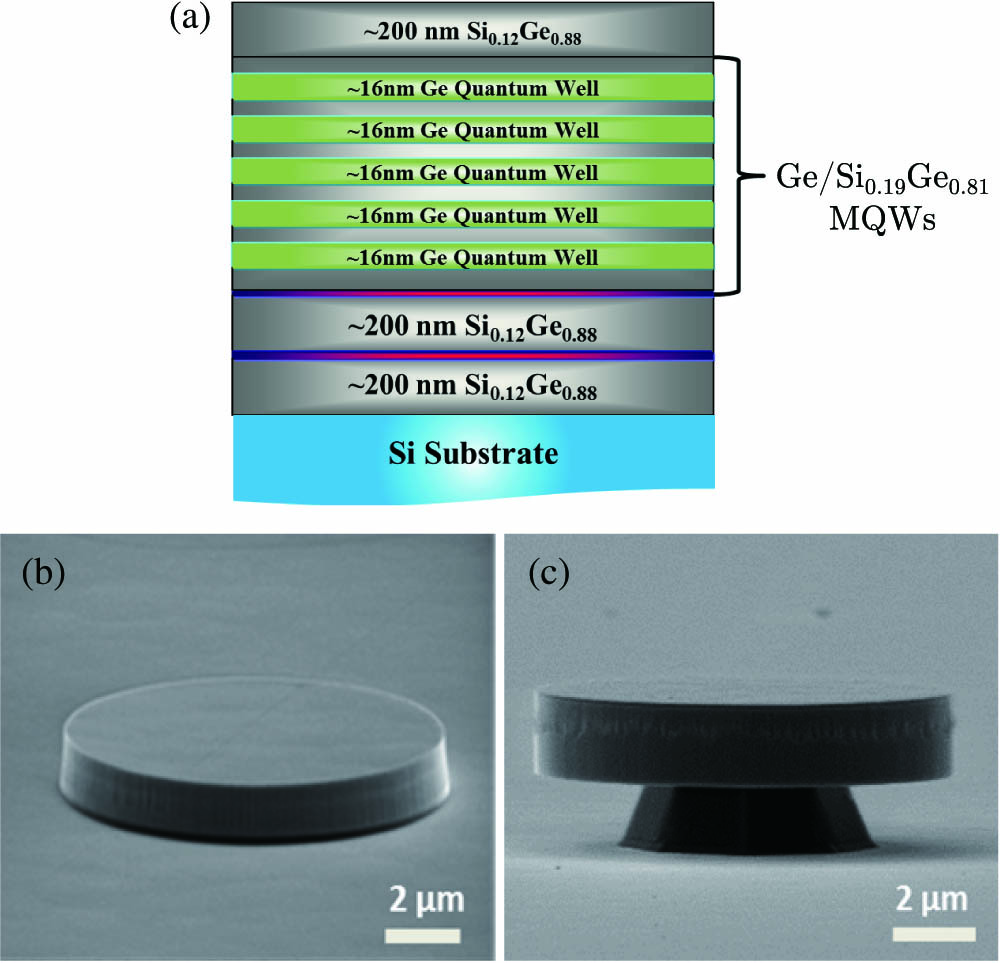
Figure 1.Epitaxial stack design and the fabricated Ge/SiGe MQW microdisks. (a) Schematic of the Ge/SiGe MQW epitaxial structure. (b) Scanning electron microscope (SEM) image of a nonsuspended Ge/SiGe MQW microdisk. (c) SEM image of a suspended Ge/SiGe MQW microdisk supported by a Si post.
The microdisks were patterned by standard optical lithography and etched into the Si substrate using in a plasma etcher, as shown in Fig. 1(b). To obtain better optical mode confinement and reduce mode leakage into the substrate, tetramethylammonium hydroxide (TMAH) was used to selectively etch the Si substrate below the Ge/SiGe MQW microdisk, leaving the SiGe buffer layer intact and suspending the microdisk on a Si post, as shown in Fig. 1(c).
PL measurements were performed using a 980 nm diode laser in a surface-normal pump and collection configuration with an extended-InGaAs detector (2.4 μm cutoff). All spectra are corrected for system response, which was calibrated using a tungsten-halogen source at a color temperature of 2960 K. Figure 2 shows the room-temperature PL spectrum of the 10 μm diameter suspended Ge/SiGe MQW microdisk from Fig. 1(c), at a pump power of 11 mW. Emission from the direct bandgap is observed at , and the signal between 1630 and 1700 nm is the tail of the indirect bandgap emission. The 50 nm blueshift in PL emission compared to bulk Ge is a result of compressive strain in the Ge QWs from the pseudomorphic growth of the Ge/SiGe MQW structure, arising from the 4% lattice mismatch between Si and Ge. Additionally, quantum confinement in the well raises the fundamental energy levels in the conduction and valence bands of Ge, also contributing to this blueshift.

Figure 2.Room-temperature PL of a suspended Ge/SiGe MQW microdisk exhibiting FP mode resonances. Inset: Bulk Ge reference showing direct bandgap emission at 1550 nm.
The PL spectrum is modulated by a series of broad resonances with a free spectral range (FSR) of , as labeled by dotted lines in Fig. 2. We attribute these resonances to Fabry–Perot (FP) modes along the diameter direction of the microdisk because the measured FSR is in agreement with the calculated value of FSR for these FP modes. Similar modes have also been observed in other Ge and GeSn microdisk cavities [17,18]. The Q factor of these resonances is , and the corresponding material loss of this microdisk is after correcting for the reflection loss. However, the compressive strain in the QWs and the defective buffer layer limit the radiative efficiency of this design and are addressed in the following section.
3. DESIGN OF TENSILE-STRAINED Ge/SiGe MQW MICRODISKS
A. Strain Simulation of Microdisks
Because compressive strain reduces light emission efficiency from the Ge QWs by further increasing the energy difference between the valley and the valley in the conduction band, the use of CMOS-compatible as a stressor is an attractive approach to introduce tensile strain into Ge [7,19–21]. The three-dimensional finite element method (3D-FEM) was used to simulate the effect of a stressor on the average in-plane biaxial strain of a suspended Ge microdisk.
We simulated the strain distributions of suspended 6 μm diameter microdisks covered with stressors (200 nm thick, initial stress) in three configurations [Fig. 3(a)]: top only (type 1), top and sidewall (type 2), and all-around (type 3). The Ge/SiGe MQW region and SiGe cap layers are approximated as a single Ge layer to reduce the computational cost of the meshing required to resolve the QWs. Because the SiGe barriers are Ge rich, average elastic properties over the entire MQW structure are comparable to Ge. The SiGe post is set to be 800 nm thick and 3 μm in diameter to mimic the undercut of the buffer layer in the actual device fabricated.
Figure 3.3D-FEM simulation for tensile-strained microdisks. (a) Schematic of type 1, type 2, and type 3 stressor configurations. (b) Cross section of the simulated strain distribution for a type 1 Ge microdisk. (c) Comparison of strain profiles for all three configurations of Ge/stressor microdisks.
Figure 3(b) shows a cross section of the simulated in-plane biaxial strain distribution of a type 1 Ge microdisk with no initial strain. After relaxation of the stressed , tensile strain is transferred from the layer to the underlying Ge layer and bends the microdisk downward at the edge (not shown in the figure) due to the vertical strain gradient. Maximum tensile strains occur near the Ge/stressor interface, but regions of increased compressive strain also exist on the opposing side. Figure 3(c) shows the comparison of the strain profiles from all three types of Ge/stressor configurations along the diameter of the microdisk at a depth of below the Ge surface, which corresponds to the position of the top Ge QW in the actual device. We observe that the biaxial strain in the center of the microdisk is higher than that at the edge for the top-only (type 1) case. This result is confirmed by Raman and PL measurements in Ref. [22]. Adding a stressor on the sidewall then enhances the strain at the edge of the microdisk. When we further add a stressor to the backside of the Ge microdisk to make an all-around stressor, more strain is transferred to the edge than to the center of the microdisk due to the added contribution of the backside stressor. This strain distribution helps accumulate carriers in the region where optical gain for the whispering gallery modes (WGMs) is needed. Therefore, we select the design of the all-around stressor (type 3) as a method of strain transfer for the Ge/SiGe MQW microdisks.
B. Tensile-Strained Ge/SiGe MQW Microdisk Fabrication
Figure 4(a) shows the new epitaxial stack for fabricating strained Ge/SiGe MQW microdisks, which differs from the initial design shown in Fig. 1(a) by the insertion of an additional etch-stop layer. Because material quality is a critical factor to achieving lasing, a relaxed buffer layer with high threading dislocation density is not desired for the microdisk stack, as it facilitates nonradiative recombination and reduces optical gain of the material. By leveraging an etch-stop layer between the buffer layer and the MQW region [23], the defective buffer layer can be removed by wet etching, leaving only the high-quality Ge/SiGe MQW region in the microdisk stack with precise thickness control. This also allows us to adopt a cavity design with a thickness of to support only the lowest-order transverse-electric (TE) and transverse-magnetic (TM) modes in the vertical direction [24]. Given the wider bandgap of used for the etch stop, this layer can further serve as a minority-carrier blocking layer to reduce surface recombination at the bottom of the microdisk.
Figure 4.(a) Schematic of the epitaxial stack of the Ge/SiGe MQW microdisk. (b) Fabrication process flow for a tensile-strained, suspended Ge/SiGe MQW microdisk. (c) SEM image of a Ge/SiGe MQW microdisk without stressor [step 8 in (b)]. (d) SEM image of a Ge/SiGe MQW microdisk with stressor [step 9 in (b)].
Following buffer growth, the 10 nm etch-stop layer was grown, which was thick enough to act as a complete etch stop without exceeding its critical thickness. Then either a 50 or 100 nm layer was grown to minimize bottom surface recombination in the microdisks as well as to symmetrize the material stack of the microdisks. Next, five 16 nm thick Ge QWs sandwiched by 25 nm thick barriers layers were grown, followed again by a 50 or 100 nm thick cap layer growth. No doping was intentionally added to any layer in the stack.
The etch-stop fabrication process of the strained Ge/SiGe MQW microdisk is illustrated in Fig. 4(b). An unstressed hard mask was deposited using plasma-enhanced chemical vapor deposition (PECVD) on top of the as-grown epitaxial stack. Standard optical lithography and -based anisotropic dry etching were used to define microdisk mesas 6 and 10 μm in diameter. Then a conformal 200 nm layer was deposited using low-pressure chemical vapor deposition followed by timed dry etching to expose the surrounding Si substrate while keeping the microdisk protected. TMAH was used to selectively etch the Si substrate laterally underneath the Ge/SiGe MQW microdisk. The defective buffer layer at the bottom of the microdisk was then etched from below using a mixture of 29% , 30% , and in a 1∶1∶10 ratio, leaving an intact high-quality Ge/SiGe MQW region with precisely controlled thickness from the etch-stop layer. The sidewall and hard mask were then removed using 6:1 buffered oxide etchant. Finally, an all-around stressor with high compressive stress was deposited on the microdisks by PECVD in a dual-frequency reactor at 350°C using 2% in He and precursors at 500 mTorr chamber pressure. The deposition conditions, including the low-frequency power, pressure, and gas flow ratio, were optimized to maximize the stress of the deposited film.
Figure 4(c) shows the scanning electron microscope (SEM) image of a 10 μm diameter suspended Ge/SiGe MQW microdisk with the SiGe buffer layer removed using the etch-stop layer technique. The SEM image of the microdisk with an all-around stressor is shown in Fig. 4(d). Note that the deposited on top of the microdisk is (target thickness), while that underneath the microdisk is . The thicknesses differ by a factor of 2 due to the geometry of the suspended microdisk and the sticking coefficients of the depositing species. Further 3D-FEM simulation shows that using an all-around (type 3) with unequal top and backside thicknesses produces a similar strain distribution as the constant thickness stressor [Fig. 3(b)], although the strain magnitude is affected. For all subsequent simulations, the thicknesses on the microdisk backside are adjusted accordingly.
C. Strain Characterization by PL and Raman Spectroscopy
Figure 5(a) shows the PL emission spectra from 10 μm diameter Ge/SiGe microdisks with the stressor and without the stressor. The emission peak in the unstrained microdisk is blueshifted compared to the spectrum shown in Fig. 2 due to the removal of the underlying buffer layer using the etch-stop technique. During epitaxial growth, a mismatch between the thermal expansion coefficients of Si and Ge results in a tensile-strained buffer layer, leading to a contraction in the Ge MQW region once it is etched away in step 7 of Fig. 4(b). The peak emission wavelength of the microdisk with 130 nm is redshifted by compared to the unstrained sample. Using deformation potential theory [25], this PL shift corresponds to an biaxial tensile strain induced by the all-around stressor. For the microdisk with 245 nm , the peak emission wavelength shows a larger redshift of , indicating that biaxial tensile strain is transferred to the microdisk. The main peak position is at 1500 nm, which is below 1550 nm due to the initial compressive strain from epitaxial growth and carrier confinement in the Ge/SiGe MQW structure.
Figure 5.PL and Raman characterizations of Ge/SiGe MQW microdisks. (a) Room-temperature PL of strained (red and blue) and unstrained (black) microdisks. (b) Typical Raman spectrum from the center of a microdisk. (c) Raman line scan along the diameter of a strained, suspended Ge/SiGe MQW microdisk.
The strain transferred from the stressor to the suspended Ge/SiGe MQW microdisks was also experimentally determined using Raman spectroscopy (HORIBA Raman system with 633 nm excitation laser and 1800 line/mm grating). A typical Raman spectrum from the center of a microdisk is shown in Fig. 5(b), in which two peaks are observed. The left peak (smaller Raman shift) is the Ge–Ge mode from the barrier and cap layers, and the right peak (larger Raman shift) is the Ge–Ge mode originating from the Ge QWs [26]. Lorentzian fitting was used to accurately determine the positions of the two peaks. By comparing the peak positions of the microdisks with and without stressors, the transferred strain from the stressor can be calculated using the Raman strain-shift coefficient of for biaxial strain in Ge [27]. Raman line scans with spatial resolution of are performed along the diameters of the microdisks with all-around , and a typical profile is shown in Fig. 5(c). The Raman results are in agreement with the simulation results, where the strain amplitude has a local minimum in the center of the microdisk. The strain reaches a maximum around 2 μm from the edge. The Raman results also show that the strain drops significantly at the edges of the microdisk. The sharp increase of the strain at the edges of the microdisk in the simulation is due to edge effects of meshing the geometry.
To systematically study the strain transfer from the all-around stressor, we investigated microdisks with different thicknesses, diameters, and stressor thicknesses using PL and Raman spectroscopy. Table 1 displays the parameters of all the microdisks that were measured. The thickness of the microdisks was tuned by modifying the thickness of the layers as shown in Fig. 4(a). The stressor thicknesses cited in Table 1 are the target deposition thicknesses on the top of the microdisks. The actual thickness underneath the microdisk is about half of the target thickness, as discussed previously. Figure 6 shows the comparisons of the simulation, PL, and Raman results for all the microdisks. The simulated strains are in good agreement with the strains from Raman measurements. In general, the strains obtained from PL measurements are lower in amplitude compared to those from simulation and Raman measurements. This is expected because the Raman and simulation data were taken at positions of maximum strain in the Raman line scan, whereas the PL measurements produced an average strain over the microdisks due to the larger spot size and deeper penetration depth of the pump laser. The highest biaxial strain transfer achieved in our design is 0.88%, which is able to compensate the original epitaxial strain in the QW and reduce the separation between and valleys by according to deformation potential theory [25]. We also find that more strain is transferred to thinner and smaller diameter microdisks compared to thicker and larger microdisks. Thicker stressors also transfer more strain to the microdisks in the regime we investigated. These results serve as a helpful guide for the future development of highly strained microstructures.
| Microdisk | Microdisk | SiNx Stressor |
| Device # | Thickness (nm) | Diameter (μm) | Thickness (nm) |
| 1 | 440 | 6 | 130 |
| 2 | 440 | 6 | 245 |
| 3 | 440 | 10 | 130 |
| 4 | 440 | 10 | 245 |
| 5 | 340 | 6 | 130 |
| 6 | 340 | 6 | 245 |
| 7 | 340 | 10 | 130 |
| 8 | 340 | 10 | 245 |
Table 1. Parameters of the Investigated Microdisks
Figure 6.Comparisons of simulation, PL, and Raman measurements. (a) Devices 1, 2 (440 nm thick, 6 μm diameter). (b) Devices 3, 4 (440 nm thick, 10 μm diameter). (c) Devices 5, 6 (340 nm thick, 6 μm diameter). (d) Devices 7, 8 (340 nm thick, 10 μm diameter).
4. OPTICAL GAIN CALCULATIONS FOR Ge/SiGe MQW
To evaluate the effects of external strain on the optical gain of the Ge/SiGe MQW structures, we performed optical gain calculations to quantify the net material gain of the Ge QWs in the Ge/SiGe MQW structures. Figure 7(a) shows the band alignment of a strain-balanced Ge QW with barriers epitaxially grown on a relaxed buffer layer [28]. In the Ge QW, to the first order, the holes can be well confined at the point where is the wave vector in reciprocal space. However, the electrons are largely confined in the valley of the conduction band where . When the valley becomes filled, the electrons begin to spill out of the QW before they are scattered to the valley, resulting in a low quantum efficiency as a light emitter for this band structure. Deformation potential calculations were conducted to model the band alignment of with 1% external biaxial tensile strain (added to the initial compressive epitaxial strain), with the results shown in Fig. 7(b). Compared to the case without external tensile strain illustrated in Fig. 7(a), the electrons in the Ge QW can be scattered to the valley before they escape out of the QW and can potentially significantly enhance the quantum efficiency of the Ge/SiGe MQW structure. For comparison, we assume the Ge QW has an n-type doping concentration of and an injection level of . These numbers are chosen to be close to the transparency condition for bulk Ge calculated in Ref. [29]. The corresponding current density in the Ge/SiGe MQWs is expected to be more than 10 times lower than bulk Ge [11]. Figure 7(c) shows the net gain spectra (gain minus free carrier absorption) for the TE mode and TM mode for Ge QWs with different external biaxial tensile strain. With 1% external biaxial tensile strain, high positive net gain of can be achieved for the TE mode at a wavelength around 1550 nm. While other methods of applying tensile strain or adding Sn to Ge extend the emission wavelength to [4,7,21], the emission and peak gain wavelength for tensile-strained Ge/SiGe MQWs remains at due to quantum confinement, which makes it compatible with optical-fiber communications.
Figure 7.Optical gain calculations for Ge/SiGe MQW. (a) Band alignment of strain-balanced MQW without external strain. (b) Band alignment of strain-balanced MQW with 1% external biaxial tensile strain. (c) TE and TM net gain spectra for Ge QW with different external biaxial tensile strain, assuming n-type doping concentration of and an injection of . Without external tensile strain, net gain is negative, meaning lasing is not achieved. As external tensile strain increases, net gain increases remarkably. Peak gain reaches positive with 1% of external tensile strain.
5. CONCLUSIONS
We discuss the design of a tensile-strained Ge/SiGe MQW microdisk, and 3D-FEM simulations suggest that a microdisk with an all-around stressor has the desired strain distribution profile for a WGM laser. We describe an etch-stop process for fabricating Ge/SiGe MQW microdisks that eliminates defective buffer layers and maintains high material quality. The strains from fabricated microdisks with different thicknesses, diameters, and stressor thicknesses are investigated using PL, Raman spectroscopy, and 3D-FEM simulations. The Raman measurements agree well with simulation results, while the PL measurements tend to yield lower strains due to an averaging effect on strains. In the thinnest (340 nm) and smallest (6 μm) microdisk with a thick stressor (245 nm), we achieved a transferred biaxial tensile strain as high as 0.88%, corresponding to an reduction of the energy separation between the and valleys. A higher strain is expected if a thicker stressor is applied. We also present optical gain calculations for the Ge/SiGe MQW and show that a high positive net gain of can be achieved for the TE mode at a wavelength of with 1% external biaxial tensile strain. These results indicate that a tensile-strained Ge/SiGe MQW microdisk with an all-around stressor is a potential candidate for efficient Ge-based lasers on Si.
Acknowledgment
Acknowledgment. This work was performed in part at the Stanford Nanofabrication Facility, which is supported by the National Science Foundation through the NNIN, and at the Stanford Nano Shared Facilities. The authors thank Dr. Robert Chen for technical discussions and Huawei Technologies for project support.
References
[1] R. E. Camacho-Aguilera, Y. Cai, N. Patel, J. T. Bessette, M. Romagnoli, L. C. Kimerling, J. Michel. An electrically pumped germanium laser. Opt. Express, 20, 11316-11320(2012).
[2] R. Chen, H. Lin, Y. Huo, C. Hitzman, T. I. Kamins, J. S. Harris. Increased photoluminescence of strain-reduced, high-Sn composition Ge1−xSnx alloys grown by molecular beam epitaxy. Appl. Phys. Lett., 99, 181125(2011).
[3] S. Al-Kabi, S. A. Ghetmiri, J. Margetis, T. Pham, Y. Zhou, W. Dou, B. Collier, R. Quinde, W. Du, A. Mosleh, J. Liu, G. Sun, R. A. Soref, J. Tolle, B. Li, M. Mortazavi, H. A. Naseem, S.-Q. Yu. An optically pumped 2.5 μm GeSn laser on Si operating at 110 K. Appl. Phys. Lett., 109, 171105(2016).
[4] S. Wirths, R. Geiger, N. Von Den Driesch, G. Mussler, T. Stoica, S. Mantl, Z. Ikonic, M. Luysberg, S. Chiussi, J. Hartmann, H. Sigg, J. Faist, D. Buca, D. Grützmacher. Lasing in direct-bandgap GeSn alloy grown on Si. Nat. Photonics, 9, 88-92(2015).
[5] M. Süess, R. Geiger, R. Minamisawa, G. Schiefler, J. Frigerio, D. Chrastina, G. Isella, R. Spolenak, J. Faist, H. Sigg. Analysis of enhanced light emission from highly strained germanium microbridges. Nat. Photonics, 7, 466-472(2013).
[6] Y. Huo, H. Lin, R. Chen, M. Makarova, Y. Rong, M. Li, T. I. Kamins, J. Vuckovic, J. S. Harris. Strong enhancement of direct transition photoluminescence with highly tensile-strained Ge grown by molecular beam epitaxy. Appl. Phys. Lett., 98, 011111(2011).
[7] A. Ghrib, M. El Kurdi, M. de Kersauson, M. Prost, S. Sauvage, X. Checoury, G. Beaudoin, I. Sagnes, P. Boucaud. Tensile-strained germanium microdisks. Appl. Phys. Lett., 102, 221112(2013).
[8] W. Tsang. Extremely low threshold (AlGa)As modified multiquantum well heterostructure lasers grown by molecular-beam epitaxy. Appl. Phys. Lett., 39, 786-788(1981).
[9] H. K. Choi, C. Wang. InGaAs/AlGaAs strained single quantum well diode lasers with extremely low threshold current density and high efficiency. Appl. Phys. Lett., 57, 321-323(1990).
[10] Y.-H. Kuo, Y. K. Lee, Y. Ge, S. Ren, J. E. Roth, T. I. Kamins, D. A. Miller, J. S. Harris. Strong quantum-confined Stark effect in germanium quantum-well structures on silicon. Nature, 437, 1334-1336(2005).
[11] E. T. Fei, X. Chen, K. Zang, Y. Huo, G. Shambat, G. Miller, X. Liu, R. Dutt, T. I. Kamins, J. Vuckovic, J. S. Harris. Investigation of germanium quantum-well light sources. Opt. Express, 23, 22424-22430(2015).
[12] K. Zang, D. Zhang, Y. Huo, X. Chen, C.-Y. Lu, E. T. Fei, T. I. Kamins, X. Feng, Y. Huang, J. S. Harris. Microring bio-chemical sensor with integrated low dark current Ge photodetector. Appl. Phys. Lett., 106, 101111(2015).
[13] P. Chaisakul, D. Marris-Morini, J. Frigerio, D. Chrastina, M.-S. Rouifed, S. Cecchi, P. Crozat, G. Isella, L. Vivien. Integrated germanium optical interconnects on silicon substrates. Nat. Photonics, 8, 482-488(2014).
[14] G. Shambat, S.-L. Cheng, J. Lu, Y. Nishi, J. Vuckovic. Direct band Ge photoluminescence near 1.6 μm coupled to Ge-on-Si microdisk resonators. Appl. Phys. Lett., 97, 241102(2010).
[15] X. Xu, T. Maruizumi, Y. Shiraki. Waveguide-integrated microdisk light-emitting diode and photodetector based on Ge quantum dots. Opt. Express, 22, 3902-3910(2014).
[16] X. Chen, Y. Huo, E. T. Fei, G. Shambat, X. Liu, T. I. Kamins, J. Vuckovic, J. S. Harris. Room temperature photoluminescence from Ge/SiGe quantum well structure in microdisk resonator. Proceedings of Symposium on Photonics and Optoelectronics, 1-3(2012).
[17] C. S. Fenrich, X. Chen, R. Chen, Y.-C. Huang, H. Chung, M.-Y. Kao, Y. Huo, T. Kamins, J. S. Harris. Strained pseudomorphic Ge1−xSnx multiple quantum well microdisk using SiNy stressor layer. ACS Photon., 3, 2231-2236(2016).
[18] R. W. Millar, K. Gallacher, J. Frigerio, A. Ballabio, A. Bashir, I. MacLaren, G. Isella, D. J. Paul. Analysis of Ge micro-cavities with in-plane tensile strains above 2%. Opt. Express, 24, 4365-4374(2016).
[19] A. Ghrib, M. De Kersauson, M. El Kurdi, R. Jakomin, G. Beaudoin, S. Sauvage, G. Fishman, G. Ndong, M. Chaigneau, R. Ossikovski, I. Sagnes. Control of tensile strain in germanium waveguides through silicon nitride layers. Appl. Phys. Lett., 100, 201104(2012).
[20] G. Capellini, C. Reich, S. Guha, Y. Yamamoto, M. Lisker, M. Virgilio, A. Ghrib, M. El Kurdi, P. Boucaud, B. Tillack, T. Schroeder. Tensile Ge microstructures for lasing fabricated by means of a silicon complementary metal-oxide-semiconductor process. Opt. Express, 22, 399-410(2014).
[21] A. Ghrib, M. El Kurdi, M. Prost, S. Sauvage, X. Checoury, G. Beaudoin, M. Chaigneau, R. Ossikovski, I. Sagnes, P. Boucaud. All-around SiN stressor for high and homogeneous tensile strain in germanium microdisk cavities. Adv. Opt. Mater., 3, 353-358(2015).
[22] M.-Y. Kao, X. Chen, Y. Huo, C. Shang, M. Xue, K. Zang, C.-Y. Lu, E. T. Fei, Y. Chen, T. I. Kamins, J. S. Harris. Tensile-strained Ge/SiGe quantum-well microdisks with overlying SiNx stressors. Conference on Lasers and Electro-Optics (CLEO), SF1P-1(2016).
[23] G. Katsaros, A. Rastelli, M. Stoffel, G. Isella, H. von Känel, A. Bittner, J. Tersoff, U. Denker, O. Schmidt, G. Costantini, K. Kern. Investigating the lateral motion of SiGe islands by selective chemical etching. Surf. Sci., 600, 2608-2613(2006).
[24] S. McCall, A. Levi, R. Slusher, S. Pearton, R. Logan. Whispering-gallery mode microdisk lasers. Appl. Phys. Lett., 60, 289-291(1992).
[25] C. Boztug, J. R. Sánchez-Pérez, F. Cavallo, M. G. Lagally, R. Paiella. Strained-germanium nanostructures for infrared photonics. ACS Nano, 8, 3136-3151(2014).
[26] O. Pages, J. Souhabi, V. Torres, A. Postnikov, K. Rustagi. Re-examination of the SiGe Raman spectra: percolation/one-dimensional-cluster scheme and ab initio calculations. Phys. Rev. B, 86, 045201(2012).
[27] F. Cerdeira, C. Buchenauer, F. H. Pollak, M. Cardona. Stress-induced shifts of first-order Raman frequencies of diamond- and zinc-blende-type semiconductors. Phys. Rev. B, 5, 580-593(1972).
[28] R. K. Schaevitz, J. E. Roth, S. Ren, O. Fidaner, D. A. Miller. Material properties of Si-Ge/Ge quantum wells. IEEE J. Sel. Top. Quantum Electron., 14, 1082-1089(2008).
[29] Y. Cai, Z. Han, X. Wang, R. E. Camacho-Aguilera, L. C. Kimerling, J. Michel, J. Liu. Analysis of threshold current behavior for bulk and quantum-well germanium laser structures. IEEE J. Sel. Top. Quantum Electron., 19, 1901009(2013).


