• Journal of Semiconductors
  • Vol. 41, Issue 1, 012101 (2020)
Huiying Zhou1, Haiping Shi2, and Baochang Cheng2、3
Author Affiliations
  • 1Computer and Information Engineering School, Central South University of Forestry and Technology, Changsha 410004, China
  • 2School of Materials Science and Engineering, Nanchang University, Nanchang 330031, China
  • 3Nanoscale Science and Technology Laboratory, Institute for Advanced Study, Nanchang University, Nanchang 330031, China
  • show less
    DOI: 10.1088/1674-4926/41/1/012101 Cite this Article
    Huiying Zhou, Haiping Shi, Baochang Cheng. Surface traps-related nonvolatile resistive switching memory effect in a single SnO2:Sm nanowire[J]. Journal of Semiconductors, 2020, 41(1): 012101 Copy Citation Text show less
    (Color online) Structure and morphology characterization of as-synthesized product. (a) XRD pattern. (b) FESEM image.
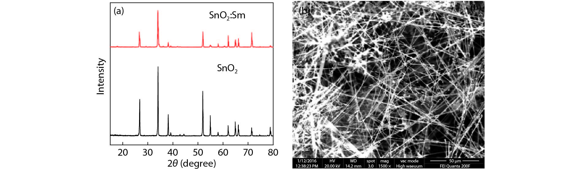
    Fig. 1. (Color online) Structure and morphology characterization of as-synthesized product. (a) XRD pattern. (b) FESEM image.
    I–V characteristics of an individual SnO2:Sm nanowire-based two-terminal device at 10 V bias voltage. (a) Typical I–V cyclic curve. The numbered arrows 1–6 indicate the direction of voltage sweeping. (b) 10 consecutive I–V cyclic curves, showing an excellent stability and repeatability.
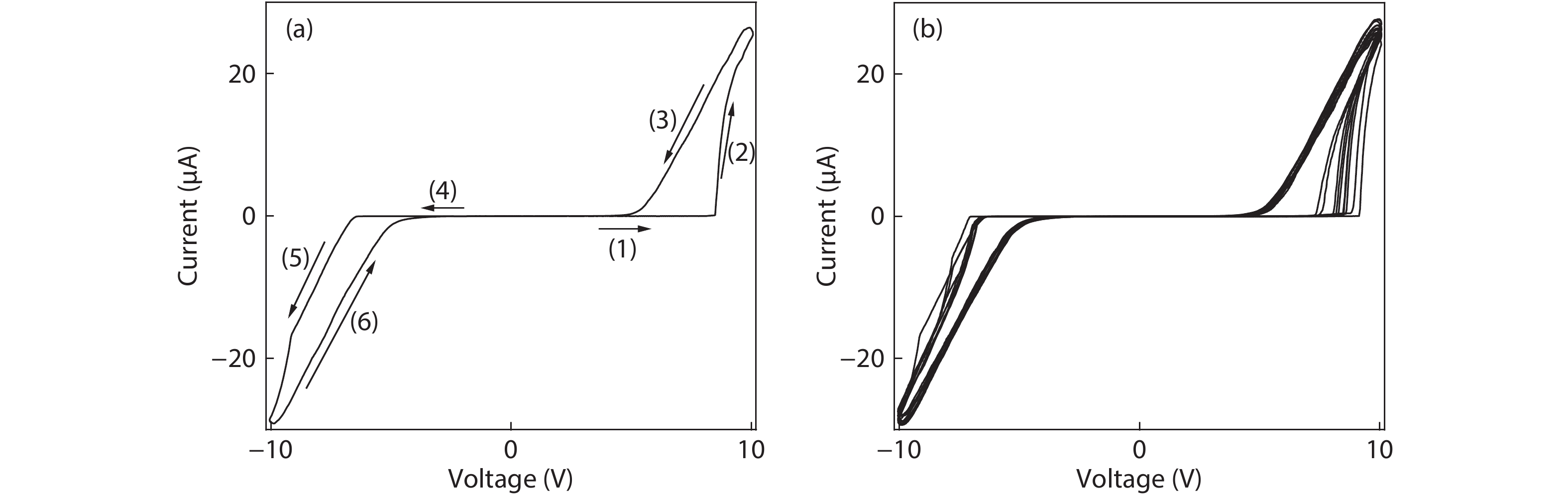
    Fig. 2. I–V characteristics of an individual SnO2:Sm nanowire-based two-terminal device at 10 V bias voltage. (a) Typical I–V cyclic curve. The numbered arrows 1–6 indicate the direction of voltage sweeping. (b) 10 consecutive I–V cyclic curves, showing an excellent stability and repeatability.
    For the step (1) and (2) curve in Fig. 2(a), the fitted plot by FN tunneling mechanism.
    Fig. 3. For the step (1) and (2) curve in Fig. 2(a), the fitted plot by FN tunneling mechanism.
    (Color online) Under only unidirectional voltage sweeping at a forward-biased bias from 0 to +10 V, I–V characteristics of an individual SnO2:Sm nanowire-based two-terminal device. (a) One typical I–V cyclic curve. (b) 10 consecutive I–V cyclic curves.
    Fig. 4. (Color online) Under only unidirectional voltage sweeping at a forward-biased bias from 0 to +10 V, I–V characteristics of an individual SnO2:Sm nanowire-based two-terminal device. (a) One typical I–V cyclic curve. (b) 10 consecutive I–V cyclic curves.
    I–V characteristics measured at a relatively low bias voltage of 2 V. (a) One I–V cyclic curve. (b) Consecutive 80 I–V cyclic curves, showing a superior repeatability.
    Fig. 5. I–V characteristics measured at a relatively low bias voltage of 2 V. (a) One I–V cyclic curve. (b) Consecutive 80 I–V cyclic curves, showing a superior repeatability.
    (Color online) Memory properties of a single nanowire-based device. (a) 7 consecutive writing-reading-erasing-reading cycles, where +6.5, +10, and –10 V are selected as reading, writing and erasing voltage, respectively. (b) An enlargement of a dotted frame in (a).
    Fig. 6. (Color online) Memory properties of a single nanowire-based device. (a) 7 consecutive writing-reading-erasing-reading cycles, where +6.5, +10, and –10 V are selected as reading, writing and erasing voltage, respectively. (b) An enlargement of a dotted frame in (a).
    (Color online) Memory properties of a single nanowire-based device. (a) 7 consecutive writing-reading-erasing-reading cycles, where +7, +10, and –10 V are selected as reading, writing and erasing voltage, respectively. (b) An enlargement of a dotted frame in (a).
    Fig. 7. (Color online) Memory properties of a single nanowire-based device. (a) 7 consecutive writing-reading-erasing-reading cycles, where +7, +10, and –10 V are selected as reading, writing and erasing voltage, respectively. (b) An enlargement of a dotted frame in (a).
    (Color online) Under different pulse voltages, the response curves of the device current. (a) Consecutive pulse between +7 and +10 V. (b) Consecutive pulse between +7 and –10 V.
    Fig. 8. (Color online) Under different pulse voltages, the response curves of the device current. (a) Consecutive pulse between +7 and +10 V. (b) Consecutive pulse between +7 and –10 V.
    (Color online) Stability of device current in LRS and HRS at a reading voltage of 6.5 V.
    Fig. 9. (Color online) Stability of device current in LRS and HRS at a reading voltage of 6.5 V.
    Huiying Zhou, Haiping Shi, Baochang Cheng. Surface traps-related nonvolatile resistive switching memory effect in a single SnO2:Sm nanowire[J]. Journal of Semiconductors, 2020, 41(1): 012101
    Download Citation