
Huiying Zhou, Haiping Shi, Baochang Cheng. Surface traps-related nonvolatile resistive switching memory effect in a single SnO2:Sm nanowire[J]. Journal of Semiconductors, 2020, 41(1): 012101
- Journal of Semiconductors
- Vol. 41, Issue 1, 012101 (2020)
Abstract
1. Introduction
For one-dimensional (1D) nanostructure semiconductors, a large number of dangling bonds can be formed owing to the damage of the lattice periodicity on their surfaces, and accordingly surface states are generated[
For wide bandgap semiconductor, the difference of electronegativity between anion and cation ions can lead to the existence of anion vacancies. These vacancies level may be very deep, resulting the formation of traps which can capture and store charges. The performance of electron transport is intensively determined by the filling and emptying of traps as well, and thus, abundant surface states and traps will play a vital role in the physical properties of nanostructures[
For the nanostructures with large specific surface area, their surface free energy is relatively high. It is very easy for doped ions to segregate on the surface to reduce free energy. The segregated doping ions can adjust the structure of surface defects, which may improve the surface-related performance of nanostructures[
Here, Sm, served as a dopant, was introduced in nanostructure SnO2. It can improve the traps in surface space charge region, resulting in a controllable storage charge effect. At the two ends connected with electrodes, their surface barriers can be reversibly modulated by the injection and extraction of electrons in the traps located in surface space charge region. A nonvolatile resistive switching (RS) memory can be obtained effectively.
2. Experiment
2.1. Sample preparation
SnO2:Sm nanowires were synthesized by an in-situ chemical vapor reaction. First, Sn(NO3)4 and SmCl3 were dissolved in deionized water. Then, a proper amount of citric acid and ethylene glycol was added to the solution. After the solution was stirred for 1 h, it was placed in an oven at 80 °C to form a sol. Subsequently, the gel was polymerized at 150 °C for 10 h. The solid resin was prepyrolyzed at 400 °C to form a Sn–Sm–C–O composite precursor.
The resulting precursor mixture was ground, and transferred to a small ceramic boat. Then, the ceramic boat is placed in the middle of a tubular furnace. After that, the tube furnace was heated to 1200 °C and kept for 2 h under N2 atmosphere. After reaction, the tubular furnace is cooled to room temperature. The white cotton-like product was obtained.
2.2. Characterization
The structure and morphology of as-synthesized product was characterized by X-ray diffraction (XRD; RIGAKU D/max-3b), and field emission environmental scanning electron microscopy (FESEM, FEI Quanta 200F), respectively.
2.3. Fabrication and electrical measurement of device
For the preparation of device, a single SnO2:Sm nanowire was transferred on an insulation substrate and then Ag electrodes were fabricated at two ends by semi-dried silver paste. Subsequently, a post-annealing was required to minimize the contact resistance under high pure N2 atmosphere at 400 °C for 10 min. Finally, the devices were packed by polydimethylsiloxane (PDMS). The electrical measurement was performed using a synthesized function generator (Stanford Research System Model DS345) and a low-noise current preamplifier (Stanford Research System Model SR570).
3. Results and discussion
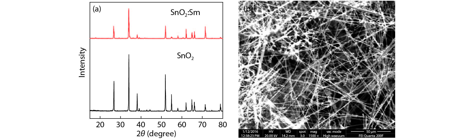
The structure and morphology of as-synthesized product were analyzed by XRD and FESEM, respectively, as shown in Fig. 1. In Fig. 1(a), all the diffraction peaks can be indexed to tetragonal rutile structure of SnO2, which is highly consistent with the standard PDF card [41-1445]. No impurity peaks were found in the diffraction patterns. From Fig. 1(b), it can be seen that the prepared sample is a non-smooth linear structure with a diameter of about 300 nm to several microns and a length of several hundred to several millimeters, indicating that wire-like one-dimension nanostructures are obtained.
![]()
Figure 1.(Color online) Structure and morphology characterization of as-synthesized product. (a) XRD pattern. (b) FESEM image.
To study the resistance properties of SnO2:Sm nanowires, I–V characteristics of a single nanowire were measured at 10 V bias voltage, as ascribed in Fig. 2. Fig. 2(a) shows a typical I–V cyclic curve. It can be seen that the device current is very small at a relatively low bias voltage, indicative of a nonconductive state. When the externally applied voltage increases to the set voltage of device, the output current suddenly increases at a voltage of about 7–8 V, and correspondingly the resistance changes from high resistance state (HRS) to low resistance state (LRS). When the voltage increases in backward direction, the same phenomenon appears as well. The I–V curve presents two symmetrical hysteresis loops with counterclockwise circulation in forward and backward directions. The device exhibits typical RS behavior at 10 V cyclic sweeping bias voltage. Fig. 2(b) shows that 10 consecutive I–V cyclic curves at 10 V bias voltage. It can be seen that the I–V curves have an excellent stability and repeatability.
![]()
Figure 2.
For the stage curve before and after current mutation, it is fitted by Fowler-Nordheim (FN) tunneling mechanism[
![]()
Figure 3.For the step (1) and (2) curve in
To further verify the relationship between RS properties and voltage polarity, the electric transport of a single nanowire-based device was measured by a unidirectional forward-biased sweeping voltage from 0 to +10 V, as illustrated in Fig. 4. It can be seen that the current varies monotonously with voltage, and the current mutation and hysteresis loop vanishes. Moreover, the back-and-forth curves can basically coincide. In addition, the threshold voltage of current increase is only about 4 V, which is lower than that of bidirectional sweeping. This result indicates that the hysteresis loop can appear only when a relatively large bidirectional sweeping voltage is applied.
![]()
Figure 4.(Color online) Under only unidirectional voltage sweeping at a forward-biased bias from 0 to +10 V,
To verify the hypothesis that the hysteresis loops come from the large reverse bias-induced polarity, the electric transport of a single nanowire-based device was further measured at a relatively low bias voltage of 2 V, as represented in Fig. 5. It can be seen that the back-and-forth curves can completely coincide. For the current mutation and hysteresis loop effect, neither do they appear as well. For the threshold voltages, moreover, there is a difference between forward and backward directions.
![]()
Figure 5.
At a relatively large cyclic bias voltage, the existence of two symmetric hysteresis loops indicates that the device has an RS feature. To investigate the RS-related memory characteristics of the individual nanowire-based device, the reading, writing and erasing performance were tested by continuous cycles, as shown in Fig. 6. The purple curve represents the loaded voltage, and the red curve corresponds to the response of current. Fig. 6(b) shows a magnified view of the dotted line frame in Fig. 6(a) which can reveal a detailed reading, writing and erasing process. The reading, writing and erasing voltages are set as +6.5, +10 and –10 V, respectively. After being applied +10 V voltage, the device resistance decreases at +6.5 V reading voltage, and conversely it increases after being applied –10 V voltage. The on/off ratio of the device current is about 230 at the reading voltage of 6.5 V. In addition, the transition speed is very fast between LRS and HRS.
![]()
Figure 6.(Color online) Memory properties of a single nanowire-based device. (a) 7 consecutive writing-reading-erasing-reading cycles, where +6.5, +10, and –10 V are selected as reading, writing and erasing voltage, respectively. (b) An enlargement of a dotted frame in (a).
To further verify the reading-writing-erasing ability of the device, +7 V reading voltage was selected for comparison, as shown in Fig. 7. The response law is the same as the above experimental result shown in Fig. 6. However, the on/off ratio of current can achieve about 940, indicating that the device has a better memory windows at 7 V reading voltage.
![]()
Figure 7.(Color online) Memory properties of a single nanowire-based device. (a) 7 consecutive writing-reading-erasing-reading cycles, where +7, +10, and –10 V are selected as reading, writing and erasing voltage, respectively. (b) An enlargement of a dotted frame in (a).
To verify the difference of device resistance at +7 V reading voltage after being applied +10 and –10 V, respectively, two different consecutive pulse voltages of (+7)–(+10) and (+7)–(–10) V were applied to test the device resistance, as shown in Fig. 8. As seen from Fig. 8(a), the device resistance is about 16 MΩ at +7 V voltage when (+7)–(+10) pulse voltage is applied. As seen from Fig. 8(b), however, the device resistance is about 4.2 MΩ at +7 V voltage when (+7)–(–10) pulse voltage is applied. Their resistances exist obvious difference at the same reading voltage after being applying a relatively large voltage with opposite direction. The results can further reveal that the device presents an LRS at a relatively low reading voltage after a relatively large bias voltage is given with the same direction, and contrarily it shows an HRS after a relatively large bias voltage is given with an opposite direction.
![]()
Figure 8.(Color online) Under different pulse voltages, the response curves of the device current. (a) Consecutive pulse between +7 and +10 V. (b) Consecutive pulse between +7 and –10 V.
To investigate the stability of SnO2:Sm nanowires memory effect, the HRS and LRS currents of device are continuously monitored at 6.5 V reading voltage, respectively, as shown in Fig. 9. It can be seen that, the HRS and LRS currents can both show a good stability after 3000 s, which firmly proves that the device has a good nonvolatile memory performance.
![]()
Figure 9.(Color online) Stability of device current in LRS and HRS at a reading voltage of 6.5 V.
For SnO2 nanowires, there are affluent surface states due to the interruption of lattice periodicity on their surfaces. Due to the electronegativity difference between Sn and O, moreover, lots of oxygen vacancies exist in SnO2 lattice, and therefore SnO2 presents n-type conductivity. For the wide bandgap SnO2, the energy level of oxygen vacancies is relatively deep, and therefore they can serve as traps centers, which can capture and store charges. Due to the existence of surface states, surface space charge region is depleted, and correspondingly the traps located in surface space region are emptied. For a single nanowire-based two-terminal device, two surface state-related back-to-back diodes are formed. At a relatively low operation bias voltage, the device is both reverse-biased for the diode connected with negative electrode, and hence it is nonconductive. With increasing operation voltage, electrons can be injected into traps located in surface space charge region from negative electrode, resulting in a decrease of surface barrier height connected with negative electrode. As a consequence, the device can conduct at a relatively large voltage. On a contrary, the electrons can be extracted from traps in surface space region into positive electrode at a relatively large operation voltage, resulting in an increase of surface barrier height connected with positive electrode. At room temperature and low operation, the trapped electrons in surface space charge region cannot be excited and injected spontaneously, and hence the modulated surface barrier height can be maintained. If a relatively low forward voltage is loaded, subsequently, the diode with a low barrier is reverse-biased, and conversely the diode with a high barrier is reverse-biased if a relatively low backward voltage is loaded. After being applied a relatively large bias, therefore, the device resistance is lower when a low forward reading voltage is loaded than that being loaded a low reverse reading voltage. After being applied a relatively large bias voltage, the sustainable asymmetry of surface barrier height leads to nonvolatile RS properties. If a relatively large reverse bias voltage is loaded, electrons can be injected into traps when the height of energy band tilting induced by electric field surpasses that of trap barrier, resulting in a reverse injection and extraction. Therefore, I–V curves can show a sudden increase companied with hysteresis loop. For the two-terminal device, the effect is reversible, and I–V curves can show two almost symmetrical hysteresis loops at forward and backward directions. For pure SnO2, surface states are complex, the nonvolatile memory effect is relatively poor. When Sm dopants are introduced into SnO2 lattice, they can easily segregate on the surface to reduce surface free energy. Moreover, Sm can exist in +3 and +4 valence. The introduction of Sm can effectively improve the traps in surface space charge region, resulting in a relatively excellent nonvolatile RS memory effect.
4. Conclusion
In summary, SnO2:Sm nanowires were prepared by an in-situ chemical vapor reaction. The introduction of Sm can improve the traps in surface space charge region. For a single nanowire-based two-terminal device, two surface state-related back-to-back diodes are formed. At a low operation bias voltage, it is nonconductive. At a relatively large voltage, however, electrons can be injected into the traps in surface space charge region from negative electrode, resulting in a decrease of surface barrier connected with negative electrode, and contrarily electrons can be extracted from the traps in surface space charge region into positive electrode, resulting in an increase of surface barrier connected with positively electrode, and contrarily electrons can be extracted from the traps in surface space charge region connected with positive electrode. The electrons in traps cannot be injected and extracted spontaneously at a relatively low operation bias voltage and room temperature. The sustainable asymmetrical surface barrier, triggered by a relatively large bias voltage, leads to a nonvolatile RS memory effect.
Acknowledgements
This work was financially supported by the National Natural Science Foundation of China (No. 51571107) and the Key Project of Hunan Provincial Department Education (No. 17A222).
References
[1] B Cheng, Z Ouyang, C Chen et al. Individual Zn2SnO4-sheathed ZnO heterostructure nanowires for efficient resistive switching memory controlled by interface states. Sci Rep, 3, 3249(2013).
[2] H Shi, B Cheng, Q Cai et al. Surface state controlled ultrahigh selectivity and sensitivity for UV photodetectors based on individual SnO2 nanowires. J Mater Chem C, 4, 8399(2016).
[3] S Barth, F Hernandez-Ramirez, J Holmes et al. Synthesis and applications of one-dimensional semiconductors. Prog Mater Sci, 55, 563(2010).
[4] F Liang, J Zhang, Z Wang et al. Broadband, ultrafast, self-driven photodetector based on Cs-doped FAPbI3 perovskite thin film. Adv Opt Mater, 5, 1700081(2017).
[5] R Devan, A Patil, J Lin et al. One-dimensional metal-oxide nanostructures: recent developments in synthesis, characterization, and applications. Adv Funct Mater, 22, 3326(2012).
[6] M Utama, J Zhang, R Chen et al. Synthesis and optical properties of II–VI 1D nanostructures. Nanoscale, 4, 1422(2012).
[7] F Wang, A Dong, W Buhro. Solution-liquid-solid synthesis, properties, and applications of one-dimensional colloidal semiconductor nanorods and nanowires. Chem Rev, 116, 10888(2016).
[8] Y Xia, P Yang, Y Sun et al. One-dimensional nanostructures: synthesis, characterization, and applications. Adv Mater, 15, 353(2003).
[9] W Ouyang, F Teng, X Fang. High performance BiOCl nanosheets/TiO2 nanotube arrays heterojunction UV photodetector: the influences of self-induced inner electric fields in the BiOCl nanosheets. Adv Funct Mater, 28, 1707178(2018).
[10] P Yu, K Hu, H Chen et al. Novel
[11] H Chen, S Yang. Hierarchical nanostructures of metal oxides for enhancing charge separation and transport in photoelectrochemical solar energy conversion systems. Nanoscale Horiz, 1, 96(2016).
[12] R LaPierre, M Robson, K Azizur-Rahman et al. A review of III–V nanowire infrared photodetectors and sensors. J Appl Phys, 50, 123001(2017).
[13] M Liu, Y Peng, Z Wu. Post-growth assembly of nanowires for integration of nanodevices. Adv Mater Res, 476–478, 1463(2012).
[14] H Zhao, Q Zhang, Y Weng. Deep surface trap filling by photoinduced carriers and interparticle electron transport observed in TiO2 nanocrystalline film with time-resolved visible and mid-IR transient spectroscopies. J Phys Chem C, 111, 3762(2007).
[15] B Cheng, J Xu, Z Ouyang et al. Individual Ohmic contacted ZnO/Zn2SnO4 radial heterostructured nanowires as photodetectors with a broad-spectral-response: injection of electrons into/from interface states. J Mater Chem C, 2, 1808(2014).
[16] S Kar, S Chaudhuri. Shape selective growth of CdS one-dimensional nanostructures by a thermal evaporation process. J Phys Chem B, 110, 4542(2006).
[17] W Tian, Y D Wang, L Chen et al. Self-powered nanoscale photodetectors. Small, 13, 1701848(2017).
[18] T Zhang, Z Li, J Wang et al. Broadband photodetector based on carbon nanotube thin film/single layer graphene Schottky junction. Sci Rep, 6, 38569(2016).
[19] B Cheng, J Zhao, L Xiao et al. PMMA interlayer-modulated memory effects by space charge polarization in resistive switching based on CuSCN nanopyramids/ZnO-nanorods p–n heterojunction. Sci Rep, 5, 17859(2015).
[20] J Zhao, B Cheng, Y Xiao et al. Ultrahigh performance negative thermal-resistance switching based on individual ZnO:K, Cl micro/nanowires for multibit nonvolatile resistance random access memory dual-written/erased repeatedly by temperature or bias. J Mater Chem C, 3, 12220(2015).
[21] J Zhao, B Cheng, Y Xiao et al. Gate-free controlled multibit memories based on individual ZnO:In micro/nanowire back-to-back diodes. Adv Electron Mater, 2, 1500395(2016).
[22] B Cheng, G Wu, Z Ouyang et al. Effects of interface states on photoexcited carriers in ZnO/Zn2SnO4 type-II radial heterostructure nanowires. ACS Appl Mater Interfaces, 6, 4057(2014).
[23] L Tao, E Cinquanta, D Chiappe et al. Cinicene field-effect transistors operating at room temperature. Nat Nanotechnol, 10, 227(2015).
[24] B Cheng, J Xu, Z Ouyang et al. Individual ZnO nanowires for photodetectors with wide response range from solar-blind ultraviolet to near-infrared modulated by bias voltage and illumination intensity. Opt Express, 21, 29719(2013).
[25] G Cadafalch Gazquez, S Lei, A George et al. Low-Cost, large-area, facile, and rapid fabrication of aligned ZnO nanowire device arrays. ACS Appl Mater Interfaces, 8, 13466(2016).
[26] T Tong, S Wang, J Zhao et al. Erasable memory properties of spectral selectivity modulated by temperature and bias in an individual CdS nanobelt-based photodetector. Nanoscale Horiz, 4, 138(2019).
[27] S Wang, J Zhao, T Tong et al. Bias-controlled tunable electronic transport with memory characteristics in an individual ZnO nanowire for realization of a self-driven UV photodetector with two symmetrical electrodes. ACS Appl Mater Interfaces, 11, 14932(2019).
[28] J Zheng, B Cheng, Fu Wu et al. Modulation of surface trap induced resistive switching by electrode annealing in individual PbS micro/nanowire-based devices for resistance random access memory. ACS Appl Mater Interfaces, 6, 20812(2014).
[29] B Cheng, X Yu, H Liu et al. Enhanced effect of electron-hole plasma emission in Dy, Li codoped ZnO nanostructures. J Appl Phys, 105, 014311(2009).
[30] Z Cheng, H B, al Zhang. Power- and energy-dependent photoluminescence of Eu3+ incorporated and segregated ZnO polycrystalline nanobelts synthesized by a facile combustion method followed by heat treatment. J Mater Chem, 20, 7821(2010).
[31] B Cheng, J Jiao, W Sun et al. Lattice variation and Raman spectroscopy in hierarchical heterostructures of zinc antimonate nanoislands on ZnO nanobelts. Nanotechnology, 21, 025704(2010).
[32]
[33]

Set citation alerts for the article
Please enter your email address
© Copyright 2018-2021 | Chinese Laser Press. All Rights Reserved 沪ICP备15018463号-20