
Wen Gu, Zhibin Liu, Yanan Guo, Xiaodong Wang, Xiaolong Jia, Xingfang Liu, Yiping Zeng, Junxi Wang, Jinmin Li, Jianchang Yan. Comprehensive study of crystalline AlN/sapphire templates after high-temperature annealing with various sputtering conditions[J]. Journal of Semiconductors, 2020, 41(12): 122802
- Journal of Semiconductors
- Vol. 41, Issue 12, 122802 (2020)
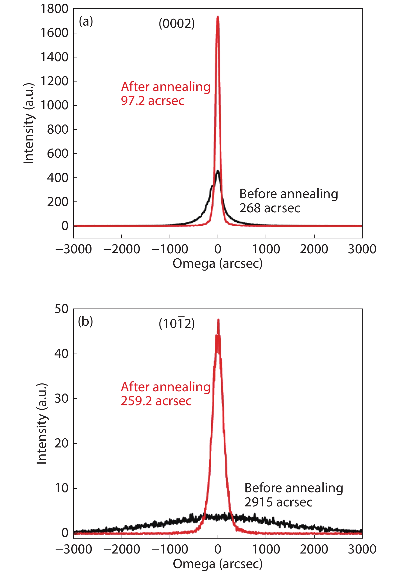
Fig. 1. (Color online) The (a) (0002)- and (b) (10
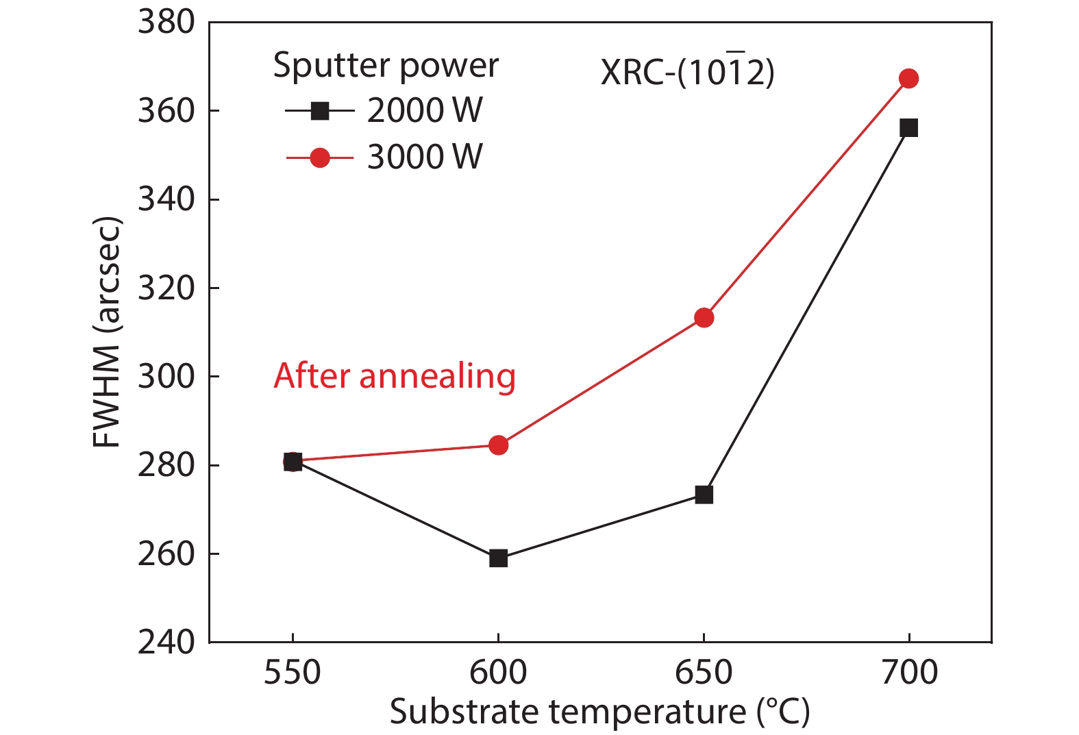
Fig. 2. (Color online) The FWHM values of (10
Fig. 3. (Color online) The (0002)-plane XRCs of the AlN films sputtered at (a) 2000 and (b) 3000 W with various substrate temperatures before HT annealing.
Fig. 4. (Color online) Raman spectrum of the AlN films sputtered at (a) 2000 and (b) 3000 W, a N2 flux of 100 sccm, and various substrate temperatures before annealing. (c) The E 2(high) peak frequency of sputtered and annealed AlN films with different substrate temperatures.
Fig. 5. (Color online) 5 × 5 μ m2 AFM images of the AlN films sputtered at 2000 W, a N2 flux of 100 sccm and substrate temperatures of (a) 550, (b) 600, (c) 650 and (d) 700 °C before annealing and (e) 550, (f) 600, (g) 650 and (h) 700 °C after annealing.
Fig. 6. The effect of N2 flux on the FWHM values of (10
Fig. 7. (Color online) The (0002)-plane XRCs of the AlN films sputtered at (a) 2000 and (b) 3000 W before annealing with various N2 fluxes.
Fig. 8. (Color online) AFM images of the AlN films sputtered at 2000 W and 600 °C with N2 fluxes of (a) 100, (b) 150 and (c) 180 sccm before annealing and (d) 100, (e) 150 and (f) 180 sccm after annealing.
|
Table 1. Sputtering parameters for the deposition of AlN films.
| ||||||||||||||||||||||||||||||||||||||||||||||||||||||||||||||||||||||||||||||||
Table 2. Characterizations for the sputtered AlN films.

Set citation alerts for the article
Please enter your email address
© Copyright 2018-2021 | Chinese Laser Press. All Rights Reserved 沪ICP备15018463号-20